Memory Hierarchy Design
Basics
The objectives of this module are to discuss about the need for a hierarchical memory system and also discuss about the different types of memories that are available.
The previous modules dealt with the Central Processing Unit (CPU), where we discussed about the Arithmetic and Logical Unit (ALU) and the control path implementation. We also looked at different techniques for improving the performance of processors by exploiting ILP. This module discusses about another component of the digital computer – viz., memory.
Whenever we look at the memory system, we would want to have fast, large and also cheap memories. Now, having all that together is not possible. Faster memories are more expensive and may also occupy more space. Therefore, having all these features together in a memory system is not practical and the only solution to reap all the benefits is to have a hierarchical memory system.
In a hierarchical memory system, the entire addressable memory space is available in the largest, slowest memory and incrementally smaller and faster memories, each containing a subset of the memory below it, proceed in steps up toward the processor. This hierarchical organization of memory works primarily because of the Principle of Locality. That is, the program accesses a relatively small portion of the address space at any instant of time. We are aware of the statement that the processor spends 90% of the time on 10% of the code. There are basically two different types of locality: temporal and spatial.
- Temporal Locality (Locality in Time): If an item is referenced, it will tend to be referenced again soon (e.g., loops, reuse)
- Spatial Locality (Locality in Space): If an item is referenced, items whose addresses are close by tend to be referenced soon (e.g., straightline code, array access) And for the past two decades or so, the hardware has relied on the principle of locality for providing speed.
Temporal and spatial locality insure that nearly all references can be found in smaller memories and at the same time gives the illusion of a large, fast memory being presented to the processor. Figure 25.1 shows a hierarchical memory system. The faster, smaller and more expensive memories are closer to the processor. As we move away from the processor, the speed decreases, cost decreases and the size increases. The registers and cache memories are closer to the processor, satisfying the speed requirements of the processor, the main memory comes next and last of all, the secondary storage which satisfies the capacity requirements. Indicated in the figure are also the typical sizes and access times of each of these types of memories. The registers which are part of the CPU itself have very low access times of a few hundreds of picoseconds and the storage space is a few thousand of bytes. The first level cache has a few kilobytes and the access times are only a few nanoseconds. The second level cache has a few hundred kilobytes and the access times increase to about 10 nanoseconds. The storage increases to a few megabytes in the case of the third level of cache, and the access times increase to a few tens of nanoseconds. The main memory has access times in the order of a few hundreds of nanoseconds, but also has larger storage. Storage is in order of terabytes for the secondary storage and the access times go to a few milliseconds. Following along the same lines, the figure also shows the memory hierarchy for a personal mobile device.
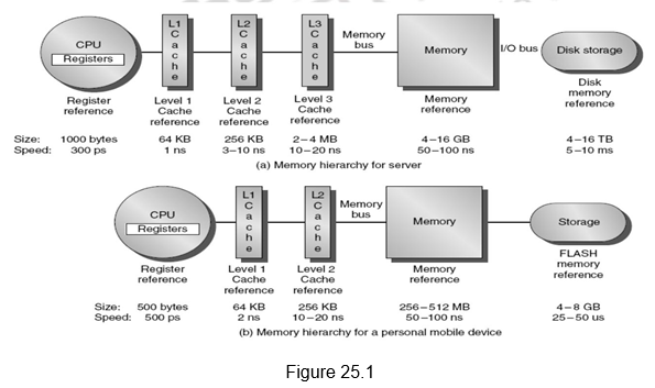
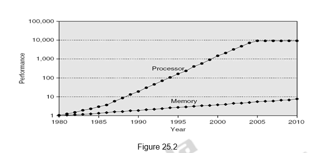
Figure 25.2 shows the memory performance gap. Although people have come up with different technological advancements to increase the speed of the processors as well as memory, the memory speeds have not kept up with the processor speeds, as indicated in Figure 25.2. The hierarchical memory system tries to hide the disparity in speed by placing the fastest memories near the processor.
Memory hierarchy design becomes more crucial with recent multi-core processors because the aggregate peak bandwidth grows with the number of cores. For example, Intel Core i7 can generate two references per core per clock. With four cores and 3.2 GHz clock, there are 25.6 billion 64-bit data references/second and 12.8 billion 128-bit instruction references= 409.6 GB/s. The DRAM bandwidth is only 6% of this (25 GB/s). Therefore, apart from a hierarchical memory system, we require different optimizations like Multi-port, pipelined caches, two levels of cache per core and shared third-level cache on chip. High-end microprocessors typically have more than 10 MB on-chip cache and it is to be noted that this consumes large amount of area and power budget.
Different types of memory: There are different types of memory available. One classification is based on the access types. A Random Access Memory (RAM) has the same access time for all locations. There are two types of RAM – Dynamic and Static RAM. Dynamic Random Access Memory has high density, consumes less power, is cheap and slow. It is called dynamic, because it needs to be “refreshed” regularly. An SRAM – Static Random Access Memory has low density, consumes high power, is expensive and fast. Here, the content will last “forever” (until power is lost). We also have “Not-so-random” Access Technology, where the access time varies from location to location and from time to time. Examples for this type of memory include disks and CDROMs. There is also one more type of memory, viz., sequential access memory where the access time is linear in location (e.g.,Tape). Normally, Dynamic RAM (DRAM) is used for main memory and Static RAM (SRAM) is used for cache.
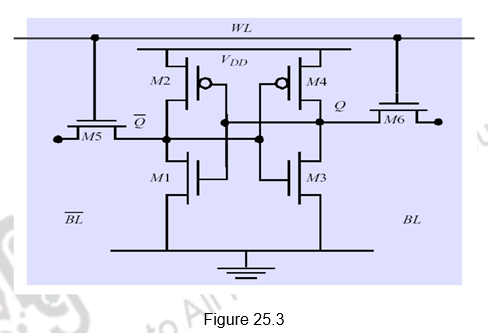
Static RAM: Figure 25.3 gives the construction of a typical SRAM cell. It requires six transistors for construction – hence the reduced density and increased cost. The six transistors are connected in a cross connected fashion. They provide regular and inverted outputs. Since it is implemented using CMOS process, it requires low power to retain the bit.
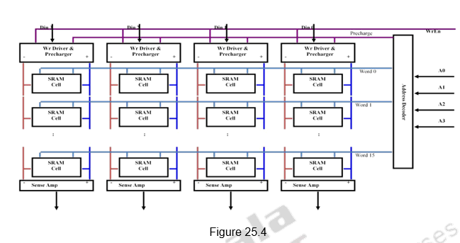
Organization of SRAM Memory: Figure 25.4 shows the single dimensional organization of an SRAM memory consisting of 16 words of 4-bits each. The four address bits are given to the address decoder which selects one of the 16 words. All bits of that word are selected. Write Enable signal is used to enable the write operation. The Data input lines are used to write fresh data into the selected word and the Data output lines are used to read data from the selected word.
Dynamic RAM: A DRAM cell is made up of a single transistor and a capacitor, as shown in Figure 25.5, leading to reduced cost and storage space. However, this is a destructive read out. It needs to be periodically refreshed, say every 8 ms., but each row can be refreshed simultaneously. For a write operation, we have to drive the bit line and select the row. For a read operation, we have to precharge the bit line to Vdd and select the row. The cell and bit line share charges and there is very small voltage change on the bit line. The sense amplifier can detect changes of ~1 million electrons. Once the read is performed, a write is to be done to restore the value. Refresh is just a dummy read to every cell. The advantage of DRAM is its structural simplicity: only one transistor and a capacitor are required per bit, compared to four or six transistors in SRAM. This allows DRAM to reach very high densities. The transistors and capacitors used are extremely small; billions can fit on a single memory chip. Due to the dynamic nature of its memory cells, DRAM consumes relatively large amounts of power, with different ways for managing the power consumption.

Figure 25.5
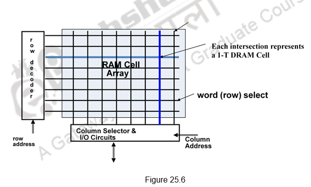
Organization of DRAM Memory: Figure 25.6 shows the two dimensional organization of DRAM. The cells are arranged as a two dimensional array. The address lines are divided into two parts – one part used for the row decoder and the other part for the column decoder. Only the cell that is selected by the row and column decoder can be read or written. As always, though the Data input and Data output lines are not shown, they are used for the Write and Read operations, respectively. In order to conserve the number of address lines, the address lines can be multiplexed. The upper half of address can be transmitted first and then the lower half of the address. The Row Address Strobe (RAS) indicates that the row address is transmitted and the Column Address Strobe (CAS) indicates that the column address is being transmitted.
Memory Optimizations: We know that even though faster memory technologies have been brought in, the speed of memory is still not comparable to the processor speeds. This is a major bottleneck. Recall Amdahl’s law which specifies that there will be a limitation on the overall performance if the common operations like memory operations are not speeded up. Memory capacity and speed should grow linearly with processor speed. However, unfortunately, memory capacity and speed has not kept pace with processors. Therefore, we can think of some optimizations to improve memory accesses. The optimizations that are normally carried out are:
- Multiple accesses to same row
- Synchronous DRAM
- Added clock to DRAM interface
- Burst mode with critical word first
- Wider interfaces
- Double data rate (DDR)
- Multiple banks on each DRAM device
Different types of DRAM: Based on the optimizations performed, there are different types of DRAMS.
Synchronous DRAM, SDRAM, is designed to synchronize itself with the timing of the CPU. This enables the memory controller to know the exact clock cycle when the requested data will be ready. Therefore, the CPU no longer has to wait between memory accesses. SDRAM chips also take advantage of interleaving and burst mode functions, which make memory retrieval even faster. SDRAM modules come in several different speeds so as to synchronize itself with the CPU’s bus they’ll be used in. The maximum speed that SDRAM will run is limited by the bus speed of the computer. SDRAM is the most common type of DRAM found in today’s personal computers. Power consumed can be reduced in SDRAMs by lowering the voltage and using the low power mode which ignores the clock and continues to refresh.
Double Data Rate SDRAM (DDR SDRAM) is a new type of SDRAM technology that supports data transfers on both edges of each clock cycle (the rising and falling edges), effectively doubling the memory chip’s data throughput. For example, with DDR SDRAM, a 100 or 133MHz memory bus clock rate yields an effective data rate of 200MHz or 266MHz. DDR SDRAM uses additional power and ground lines and requires 184-pin DIMM modules rather than the 168-pin DIMMs used by SDRAM. DDR SDRAM also consumes less power, which makes it well suited to notebook computers.
Direct Rambus DRAM (RDRAM) is a new DRAM architecture and interface standard that challenges traditional main memory designs. It transfers data at speeds up to 800MHz over a narrow 16-bit bus called a Direct Rambus Channel. This high-speed clock rate is possible due to a feature called “double clocked,” which allows operations to occur on both the rising and falling edges of the clock cycle. Rambus is designed to fit into existing motherboard standards. The components that are inserted into motherboard connections are called Rambus in-line memory modules (RIMMs). They replace conventional DIMMs. DDR SDRAM and RDRAM compete in the high performance end of the microcomputer market. Because of its new architecture a RDRAM system is somewhat more expensive than DDR SDRAM. Many computer companies make high-end microcomputers with both memory systems and let the consumer make their choice.
Graphics double data rate SDRAM (GDDR SDRAM) is a type of specialized DDR SDRAM designed to be used as the main memory of graphics processing units (GPUs). GDDR SDRAM is distinct from commodity types of DDR SDRAM such as DDR3, although they share some core technologies. Their primary characteristics are higher clock frequencies for both the DRAM core and I/O interface, which provides greater memory bandwidth for GPUs. As of 2015, there are four successive generations of GDDR: GDDR2, GDDR3, GDDR4, and GDDR5.
Read Only Memory (ROM) is a type of non-volatile memory used in computers and other electronic devices. Data stored in ROM can only be modified slowly, with difficulty, or not at all, so it is mainly used to store firmware, as BIOS of desktop computers and in embedded devices (also serves as a code protection device). We have ROMs that are read-only in normal operation, but can still be reprogrammed in some way. Erasable programmable read-only memory (EPROM) and electrically erasable programmable read-only memory (EEPROM) can be erased and re-programmed, but usually this can only be done at relatively slow speeds, may require special equipment to achieve, and is typically only possible a certain number of times.
Flash memory is an electronic non-volatile computer storage medium that can be electrically erased and reprogrammed. It is a type of EEPROM. It must be erased (in blocks) before being overwritten. It has limited number of write cycles. It is cheaper than SDRAM, but more expensive than disk. It is slower than SRAM, and faster than disk. It is extensively used in PDAs, digital audio players, digital cameras, mobile phones, etc. Its mechanical shock resistance is the reason for its popularity over hard disks in portable devices, as also its high durability, being able to withstand high pressure, temperature, immersion in water, etc.
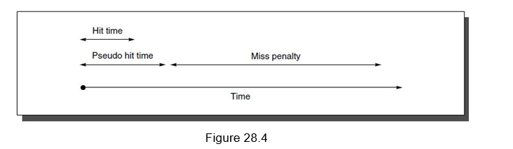
Memory hierarchy terminology: Let us now look at the terminology that is used with a hierarchical memory system. A Hit is said to occur if data appears in some block in the upper level. Hit Rate is the fraction of memory access found in the upper level and Hit Time is the time to access the upper level which consists of RAM access time + Time to determine hit/miss. A Miss is said to occur if data needs to be retrieved from a block in the lower level. Miss Rate = 1 – (Hit Rate). Miss Penalty is the time to replace a block in the upper level + Time to deliver the block to the processor. Hit Time is normally Miss Penalty. When a word is not found in the cache, a miss occurs:
• Fetch word from lower level in hierarchy, requiring a higher latency reference
• Lower level may be another cache or the main memory
• Also fetch the other words contained within the block
• Takes advantage of spatial locality
Performance Metrics: Latency is a concern of cache and bandwidth is a concern of multiprocessors and I/O. The access time is the time between read request and when desired word arrives. The Cycle time is the minimum time between unrelated requests to memory.
Example to show the impact on performance: Suppose a processor executes at a Clock Rate = 200 MHz (5 ns per cycle) with a CPI = 1.1 and with 50% arithmetic/logical, 30% load/store, 20% control instructions. Suppose that 10% of memory operations get 50 cycle miss penalty.
| Ideal CPI | 1.1 |
| Data Miss | 1.5 |
| Inst Miss | 0.5 |
CPI = ideal CPI + average stalls per instruction= 1.1(cycles) + ( 0.30 (datamops/ins) x 0.10 (miss/datamop) x 50 (cycle/miss) )
= 1.1 cycle + 1.5 cycle = 2. 6
This shows that 58 % of the time the processor is stalled waiting for memory! Adding a a 1% instruction miss rate would add an additional 0.5 cycles to the CPI.
This shows us how important the memory hierarchy design is. The data transfer between registers and memory is managed by the compiler and programmer. The data transfer between cache and memory is managed by the hardware. And the transfer between the memory and disks is managed by the hardware and operating system (virtual memory) and by the programmer (files).
To summarize, a hierarchical memory system is needed to meet the speed, capacity and cost requirements. There are two different types of locality exploited:
– Temporal Locality (Locality in Time): If an item is referenced, it will tend to be referenced again soon
– Spatial Locality (Locality in Space): If an item is referenced, items whose addresses are close by tend to be referenced soon
By taking advantage of the principle of locality, we present the user with as much memory as is available in the cheapest technology and provide access at the speed offered by the fastest technology. SRAMs and DRAMs are very useful as cache and main memory, respectively. Other types of memories like ROM and Flash memories are also very useful. DRAM is slow but cheap and dense. It is a good choice for presenting the user with a BIG memory system. SRAM is fast but expensive and not very dense and is a good choice for providing the user FAST access time.
Web Links / Supporting Materials
- Computer Organization and Design – The Hardware / Software Interface, David A. Patterson and John L. Hennessy, 4th Edition, Morgan Kaufmann, Elsevier, 2009.
- Computer Architecture – A Quantitative Approach , John L. Hennessy and David A.Patterson, 5th Edition, Morgan Kaufmann, Elsevier, 2011.
- Computer Organization, Carl Hamacher, Zvonko Vranesic and Safwat Zaky, 5th.Edition, McGraw- Hill Higher Education, 2011.
Basics of Cache Memory
The objectives of this module are to discuss about the basics of cache memories. We will discuss about the various mapping policies and also discuss about the read/write policies. Basically, the four primary questions with respect to block placement, block identification, block replacement and write strategy will be answered.
The speed of the main memory is very low in comparison with the speed of modern processors. For good performance, the processor cannot spend much of its time waiting to access instructions and data in main memory. Hence, it is important to devise a scheme that reduces the time needed to access the necessary information. Since the speed of the main memory unit is limited by electronic and packaging constraints, the solution must be sought in a different architectural arrangement. An efficient solution is to use a fast cache memory*,* which essentially makes the main memory appear to the processor to be faster than it really is. The cache is a smaller, faster memory which stores copies of the data from the most frequently used main memory locations. As long as most memory accesses are to cached memory locations, the average latency of memory accesses will be closer to the cache latency than to the latency of main memory.
The effectiveness of the cache mechanism is based on a property of computer programs called locality of reference. Analysis of programs shows that most of their execution time is spent on routines in which many instructions are executed repeatedly. These instructions may constitute a simple loop, nested loops, or a few procedures that repeatedly call each other. The actual detailed pattern of instruction sequencing is not important – the point is that many instructions in localized areas of the program are executed repeatedly during some time period, and the remainder of the program is accessed relatively infrequently. This is referred to as locality of reference*.* It manifests itself in two ways: temporal and spatial. The first means that a recently executed instruc-tion is likely to be executed again very soon. The spatial aspect means that instructions in close proximity to a recently executed instruction (with respect to the instructions’ addresses) are also likely to be executed soon.
If the active segments of a program can be placed in a fast cache memory, then the total execution time can be reduced significantly. Conceptually, operation of a cache memory is very simple. The memory control circuitry is designed to take advantage of the property of locality of reference. The temporal aspect of the locality of reference suggests that whenever an information item (instruction or data) is first needed, this item should be brought into the cache where it will hopefully remain until it is needed again. The spatial aspect suggests that instead of fetching just one item from the main memory to the cache, it is useful to fetch several items that reside at adjacent addresses as well. We will use the term block to refer to a set of contiguous address locations of some size. Another term that is often used to refer to a cache block is cache line.
The cache memory that is included in the memory hierarchy can be split or unified/dual. A split cache is one where we have a separate data cache and a separate instruction cache. Here, the two caches work in parallel, one transferring data and the other transferring instructions. A dual or unified cache is wherein the data and the instructions are stored in the same cache. A combined cache with a total size equal to the sum of the two split caches will usually have a better hit rate. This higher rate occurs because the combined cache does not rigidly divide the number of entries that may be used by instructions from those that may be used by data. Nonetheless, many processors use a split instruction and data cache to increase cache bandwidth.
When a Read request is received from the processor, the contents of a block of memory words containing the location specified are transferred into the cache. Subsequently, when the program references any of the locations in this block, the desired contents are read directly from the cache. Usually, the cache memory can store a reasonable number of blocks at any given time, but this number is small compared to the total number of blocks in the main memory. The correspondence between the main memory blocks and those in the cache is specified by a mapping function. When the cache is full and a memory word (instruction or data) that is not in the cache is referenced, the cache control hardware must decide which block should be removed to create space for the new block that contains the referenced word. The collection of rules for making this decision constitutes the replacement algorithm.
Therefore, the three main issues to be handled in a cache memory are
· Cache placement – where do you place a block in the cache?
· Cache identification – how do you identify that the requested information is available in the cache or not?
· Cache replacement – which block will be replaced in the cache, making way for an incoming block?
These questions are answered and explained with an example main memory size of 1MB (the main memory address is 20 bits), a cache memory of size 2KB and a block size of 64 bytes. Since the block size is 64 bytes, you can immediately identify that the main memory has 214 blocks and the cache has 25 blocks. That is, the 16K blocks of main memory have to be mapped to the 32 blocks of cache. There are three different mapping policies – direct mapping, fully associative mapping and n-way set associative mapping that are used. They are discussed below.
Direct Mapping: This is the simplest mapping technique. In this technique, block i of the main memory is mapped onto block j modulo (number of blocks in cache) of the cache. In our example, it is block j mod 32. That is, the first 32 blocks of main memory map on to the corresponding 32 blocks of cache, 0 to 0, 1 to 1, … and 31 to 31. And remember that we have only 32 blocks in cache. So, the next 32 blocks of main memory are also mapped onto the same corresponding blocks of cache. So, 32 again maps to block 0 in cache, 33 to block 1 in cache and so on. That is, the main memory blocks are grouped as groups of 32 blocks and each of these groups will map on to the corresponding cache blocks. For example, whenever one of the main memory blocks 0, 32, 64, … is loaded in the cache, it is stored only in cache block 0. So, at any point of time, if some other block is occupying the cache block, that is removed and the other block is stored. For example, if we want to bring in block 64, and block 0 is already available in cache, block 0 is removed and block 64 is brought in. Similarly, blocks 1, 33, 65, … are stored in cache block 1, and so on. You can easily see that 29 blocks of main memory will map onto the same block in cache. Since more than one memory block is mapped onto a given cache block position, contention may arise for that position even when the cache is not full. That is, blocks, which are entitled to occupy the same cache block, may compete for the block. For example, if the processor references instructions from block 0 and 32 alternatively, conflicts will arise, even though the cache is not full. Contention is resolved by allowing the new block to overwrite the currently resident block. Thus, in this case, the replacement algorithm is trivial. There is no other place the block can be accommodated. So it only has to replace the currently resident block.
Placement of a block in the cache is determined from the memory address. The memory address can be divided into three fields, as shown in Figure 26.1. The low-order 6 bits select one of 64 words in a block. When a new block enters the cache, the 5-bit cache block field determines the cache position in which this block must be stored. The high-order 9 bits of the memory address of the block are stored in 9 tag bits associated with its location in the cache. They identify which of the 29 blocks that are eligible to be mapped into this cache position is currently resident in the cache. As a main memory address is generated, first of all check the block field. That will point to the block that you have to check for. Now check the tag field. If they match, the block is available in cache and it is a hit. Otherwise, it is a miss. Then, the block containing the required word must first be read from the main memory and loaded into the cache. Once the block is identified, use the word field to fetch one of the 64 words. Note that the word field does not take part in the mapping.
Figure 26.1 Direct mapping
Consider an address 78F28 which is 0111 1000 1111 0010 1000. Now to check whether the block is in cache or not, split it into three fields as 011110001 11100 101000. The block field indicates that you have to check block 28. Now check the nine bit tag field. If they match, it is a hit.
The direct-mapping technique is easy to implement. The number of tag entries to be checked is only one and the length of the tag field is also less. The replacement algorithm is very simple. However, it is not very flexible. Even though the cache is not full, you may have to do a lot of thrashing between main memory and cache because of the rigid mapping policy.
Fully Associative Mapping: This is a much more flexible mapping method, in which a main memory block can be placed into any cache block position. This indicates that there is no need for a block field. In this case, 14 tag bits are required to identify a memory block when it is resident in the cache. This is indicated in Figure 5.8. The tag bits of an address received from the processor are compared to the tag bits of each block of the cache to see if the desired block is present. This is called the associative-mapping technique. It gives complete freedom in choosing the cache location in which to place the memory block. Thus, the space in the cache can be used more efficiently. A new block that has to be brought into the cache has to replace (eject) an existing block only if the cache is full. In this case, we need an algorithm to select the block to be replaced. The commonly used algorithms are random, FIFO and LRU. Random replacement does a random choice of the block to be removed. FIFO removes the oldest block, without considering the memory access patterns. So, it is not very effective. On the other hand, the least recently used technique considers the access patterns and removes the block that has not been referenced for the longest period. This is very effective.
Thus, associative mapping is totally flexible. But, the cost of an associative cache is higher than the cost of a direct-mapped cache because of the need to search all the tag patterns to determine whether a given block is in the cache. This should be an associative search as discussed in the previous section. Also, note that the tag length increases. That is, both the number of tags and the tag length increase. The replacement also is complex. Therefore, it is not practically feasible.
Figure 26.2 Fully associative mapping
Set Associative Mapping: This is a compromise between the above two techniques. Blocks of the cache are grouped into sets, consisting of n blocks, and the mapping allows a block of the main memory to reside in any block of a specific set. It is also called n-way set associative mapping. Hence, the contention problem of the direct method is eased by having a few choices for block placement. At the same time, the hardware cost is reduced by decreasing the size of the associative search. For our example, the main memory address for the set-associative-mapping technique is shown in Figure 26.3 for a cache with two blocks per set (2–way set associative mapping). There are 16 sets in the cache. In this case, memory blocks 0, 16, 32 … map into cache set 0, and they can occupy either of the two block positions within this set. Having 16 sets means that the 4-bit set field of the address determines which set of the cache might contain the desired block. The 11 bit tag field of the address must then be associatively compared to the tags of the two blocks of the set to check if the desired block is present. This two-way associative search is simple to implement and combines the advantages of both the other techniques. This can be in fact treated as the general case; when n is 1, it becomes direct mapping; when n is the number of blocks in cache, it is associative mapping.
Figure 26.3 Set associative mapping
One more control bit, called the valid bit*,* must be provided for each block. This bit indicates whether the block contains valid data. It should not be confused with the modified, or dirty, bit mentioned earlier. The dirty bit, which indicates whether the block has been modified during its cache residency, is needed only in systems that do not use the write-through method. The valid bits are all set to 0 when power is initially applied to the system or when the main memory is loaded with new programs and data from the disk. Transfers from the disk to the main memory are carried out by a DMA mechanism. Normally, they bypass the cache for both cost and performance reasons. The valid bit of a particular cache block is set to 1 the first time this block is loaded from the main memory, Whenever a main memory block is updated by a source that bypasses the cache, a check is made to determine whether the block being loaded is currently in the cache. If it is, its valid bit is cleared to 0. This ensures that stale data will not exist in the cache.
A similar difficulty arises when a DMA transfer is made from the main memory to the disk, and the cache uses the write-back protocol. In this case, the data in the memory might not reflect the changes that may have been made in the cached copy. One solution to this problem is to flush the cache by forcing the dirty data to be written back to the memory before the DMA transfer takes place. The operating system can do this easily, and it does not affect performance greatly, because such disk transfers do not occur often. This need to ensure that two different entities (the processor and DMA subsystems in this case) use the same copies of data is referred to as a cache-coherence problem.
Read / write policies: Last of all, we need to also discuss the read/write policies that are followed. The processor does not need to know explicitly about the existence of the cache. It simply issues Read and Write requests using addresses that refer to locations in the memory. The cache control circuitry determines whether the requested word currently exists in the cache. If it does, the Read or Write operation is performed on the appropriate cache location. In this case, a read or write hit is said to have occurred. In a Read operation, no modifications take place and so the main memory is not affected. For a write hit, the system can proceed in two ways. In the first technique, called the write-through protocol, the cache location and the main memory location are updated simultaneously. The second technique is to update only the cache location and to mark it as updated with an associated flag bit, often called the dirty or modified bit. The main memory location of the word is updated later, when the block containing this marked word is to be removed from the cache to make room for a new block. This technique is known as the write-back, or copy-back protocol. The write-through protocol is simpler, but it results in unnecessary write operations in the main memory when a given cache word is updated several times during its cache residency. Note that the write-back protocol may also result in unnecessary write operations because when a cache block is written back to the memory all words of the block are written back, even if only a single word has been changed while the block was in the cache. This can be avoided if you maintain more number of dirty bits per block. During a write operation, if the addressed word is not in the cache, a write miss occurs. Then, if the write-through protocol is used, the information is written directly into the main memory. In the case of the write-back protocol, the block containing the addressed word is first brought into the cache, and then the desired word in the cache is overwritten with the new information.
When a write miss occurs, we use the write allocate policy or no write allocate policy. That is, if we use the write back policy for write hits, then the block is anyway brought to cache (write allocate) and the dirty bit is set. On the other hand, if it is write through policy that is used, then the block is not allocated to cache and the modifications happen straight away in main memory.
Irrespective of the write strategies used, processors normally use a write buffer to allow the cache to proceed as soon as the data is placed in the buffer rather than wait till the data is actually written into main memory.
To summarize, we have discussed the need for a cache memory. We have examined the various issues related to cache memories, viz., placement policies, replacement policies and read / write policies. Direct mapping is the simplest to implement. In a direct mapped cache, the cache block is available before determining whether it is a hit or a miss, as it is possible to assume a hit and continue and recover later if it is a miss. It also requires only one comparator compared to N comparators for n-way set associative mapping. In the case of set associative mapping, there is an extra MUX delay for the data and the data comes only after determining whether it is hit or a miss. However, the operation can be speeded up by comparing all the tags in the set in parallel and selecting the data based on the tag result. Set associative mapping is more flexible than direct mapping. Full associative mapping is the most flexible, but also the most complicated to implement and is rarely used.
Web Links / Supporting Materials
- Computer Organization and Design – The Hardware / Software Interface, David A. Patterson and John L. Hennessy, 4th Edition, Morgan Kaufmann, Elsevier, 2009.
- Computer Architecture – A Quantitative Approach , John L. Hennessy and David A.Patterson, 5th Edition, Morgan Kaufmann, Elsevier, 2011.
- Computer Organization, Carl Hamacher, Zvonko Vranesic and Safwat Zaky, 5th.Edition, McGraw- Hill Higher Education, 2011.
Cache Optimizations I
The objectives of this module are to discuss the various factors that contribute to the average memory access time in a hierarchical memory system and discuss some of the techniques that can be adopted to improve the same.
The previous module discussed the need for a hierarchical memory system to meet the speed, capacity and cost requirements of the processor and how a cache memory can be used to hide the latency associated with the main memory access. We also looked at the various mapping policies and read / write policies adopted in cache memories.
Memory Access Time: In order to look at the performance of cache memories, we need to look at the average memory access time and the factors that will affect it. The average memory access time (AMAT) is defined as
AMAT = htc + (1 – h) (tm + tc), where tc in the second term is normally ignored.
h : hit ratio of the cache
tc : cache access time
1 – h : miss ratio of the cache
tm : main memory access time
AMAT can be written as hit time + (miss rate x miss penalty). Reducing any of these factors reduces AMAT. You can easily observe that as the hit ratio of the cache nears 1 (that is 100%), all the references are to the cache and the memory access time is governed only by the cache system. Only the cache performance matters then. On the other hand, if we miss in the cache, the miss penalty, which is the main memory access time also matters. So, all the three factors contribute to AMAT and optimizations can be carried out to reduce one or more of these parameters.
There are different methods that can be used to reduce the AMAT. There are about eighteen different cache optimizations that are organized into 4 categories as follows:
Ø Reducing the miss penalty:
§ Multilevel caches, critical word first, giving priority to read misses over write misses, merging write buffer entries, and victim caches
Ø Reducing the miss rate
§ Larger block size, larger cache size, higher associativity, way prediction and pseudo associativity, and compiler optimizations
Ø Reducing the miss penalty or miss rate via parallelism
§ Non-blocking caches, Multi banked caches, hardware & compiler prefetching
Ø Reducing the time to hit in the cache
§ Small and simple caches, avoiding address translation, pipelined cache access, and trace caches
In this module, we shall discuss the techniques that can be used to reduce the miss penalty. The time to handle a miss is becoming more and more the controlling factor. This is because of the great improvement in the speed of processors as compared to the speed of memory. Five optimizations that can be used to address the problem of improving Miss Penalty are:
• Multi-level caches
• Critical Word First and Early Restart
• Giving Priority to Read Misses over Writes
• Merging Write Buffer
• Victim Caches
We shall examine each of these in detail.
Multi-level Caches: The first techniques that we discuss and one of the most widely used techniques is using multi-level caches, instead of a single cache. When we have a single level of cache, we should decide on whether to make the cache faster to keep pace with the CPUs, or make the cache larger to overcome the widening gap between the CPU and the main memory. Both these can be handled by introducing one more level of cache. Thus, adding another level of cache between the original cache and memory simplifies the decision. The first-level cache can be small enough to match the clock cycle time of the fast CPU. Yet, the second level cache can be large enough to capture many accesses that would go to main memory, thereby lessening the effective miss penalty.
Using two levels of caches, the AMAT will have to be changed appropriately. Using the subscripts L1 and L2 to refer, respectively, to a first-level and a second-level cache, the original formula is
Average Memory Access Time = Hit TimeL1 + Miss RateL1 x Miss PenaltyL1 But, Miss PenaltyL1 = Hit TimeL2 + Miss RateL2 x Miss PenaltyL2
Therefore, Average Memory Access Time = Hit TimeL1 + Miss RateL1 x (Hit TimeL2 + Miss RateL2 x Miss PenaltyL2)
We can define two different miss rates – local miss rate and global miss rate. Local miss rate—Number of misses in a cache divided by the total number of memory accesses to this cache (Miss rateL2). Global miss rate—Number of misses in the cache divided by the total number of memory accesses generated by the CPU (Miss RateL1 x Miss RateL2).
The local miss rate is large for second-level caches because the first-level cache skims the cream of the memory accesses. This is why the global miss rate is a more useful measure: It indicates what fraction of the memory accesses that leave the processor go all the way to memory. However, the disadvantage is that it requires extra hardware.
Figure 27.1 gives the miss rates versus the cache size for multilevel caches. It can be observed that the global cache miss rate is very similar to the single cache miss rate of the second-level cache, provided that the second-level cache is much larger than the first-level cache. The miss rate of the second level cache is a function of the miss rate of the first level cache, and hence can vary by changing the first-level cache. Thus, the global cache miss rate should be used when evaluating second-level caches.
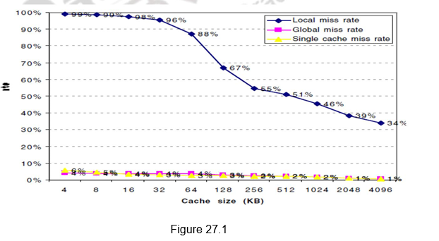
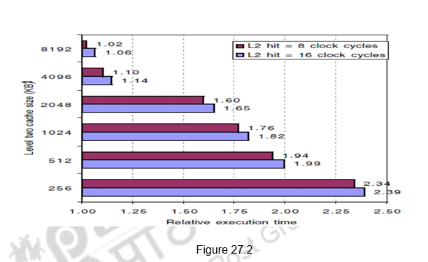
Figure 27.2 shows the relative execution times versus the second level cache size. Observe that the speed of the first-level cache affects the clock rate of the processor, while the speed of the second-level cache only affects the miss penalty of the first-level cache. A major decision is the size of a second-level cache. Since everything in the first-level cache is likely to be in the second-level cache, the second-level cache should be much bigger than the first. If second-level caches are just a little bigger, the local miss rate will be high. This observation inspires the design of huge second-level caches. Also, improving the associativity of the second-level cache will improve performance.
Early Restart and Critical Word First: This technique is based on the observation that the processor normally may need just one word of the block at a time, indicating that we don’t have to wait for the full block to be loaded before sending the requested word and restarting the processor. There are two specific strategies:
Critical word first—Request the exact word from memory and send it to the processor as soon as it arrives so that the processor continues execution as the rest of the words in the block are read. It is also called wrapped fetch and requested word first.
Early restart—Fetch the words in normal order, but as soon as the requested word of the block arrives, send it to the processor and let the processor continue execution.
Generally, these techniques only benefit designs with large cache blocks, since the benefit is low for small blocks. Note that caches normally continue to satisfy accesses to other blocks while the rest of the block is being filled. With spatial locality, there is a good chance that the next reference is to the rest of the block and the miss penalty is not very simple to calculate. When there is a second request in critical word first, the effective miss penalty is the non-overlapped time from the reference until the second piece arrives. Thus, the benefits of critical word first and early restart depend on the size of the block and the likelihood of another access to the portion of the block that has not yet been fetched.
Giving Priority to Read Misses over Writes: In the previous module, we have pointed out the usage of a write buffer. The data to be written into main memory is written into the write buffer and the processor access continues. The optimization proposed here is normally done with a write buffer. Write buffers, however, do complicate memory accesses because they might hold the updated value of a location needed on a read miss. This will lead to RAW hazards. The simplest way to handle this is for the read miss to wait until the write buffer is empty. The other alternative is to check the contents of the write buffer on a read miss, and if there are no conflicts and the memory system is available, allow the read miss to continue. Most of the processors use the second approach, thus, giving reads priority over writes.
This optimization can be effective for write back caches also. Suppose a read miss has to replace a dirty memory block. Instead of writing the dirty block to memory, and then reading memory, we could copy the dirty block to the write buffer, then read memory, and then write memory. This way the processor read will finish faster. However, RAW hazards will have to handled appropriately.
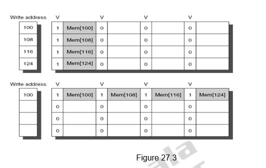
Merging Write Buffer Entries: This is an optimization used to improve the efficiency of write buffers. Normally, if the write buffer is empty, the data and the full address will be written in the buffer. The CPU continues working, while the buffer prepares to write the word to the memory. Now, if the buffer contains other modified blocks, the addresses can be checked to see if the address of this new data matches the address of a valid write buffer entry. If so, the new data can be combined with the already available entry, called write merging. This is illustrated in Figure 27.3. The first diagram shows the write buffer entries without merging. The second diagram shows the effect of merging of.the write buffer entries. Addresses 100, 108, 116 and 124 are consecutive addresses and so they have been merged into one entry.
This optimization uses the memory more efficiently since multiword writes are usually faster than writes performed one word at a time. Also it reduces the stalls due to the write buffer being full. If the write buffer had been full and there had been no address match, the cache (and CPU) must wait until the buffer has an empty entry. The Sun Niagara processor is one of the processors that uses write merging. However, I/O addresses cannot allow write merging because separate I/O registers may not act like an array of words in memory.
Victim Cache: The last technique that we discuss in this module to reduce miss penalty is the use of a victim cache. One approach to lower the miss penalty is to remember what was discarded in case it is needed again. For example, in the direct mapping, if the discarded block is again needed. Such recycling requires a small, fully associative cache between a cache and its refill path – called the victim cache, because it stores the victims of the eviction policy. The victim cache contains only the blocks that are discarded from a cache because of a miss – ―victims‖ – and are checked on a miss to see if they have the desired data before going to the next lower-level memory. If it is found, then the victim block and the cache block are swapped. Figure 27.4 shows the placement of the victim cache.
Normally, in a write back cache, the block that is replaced is sometimes called the victim. Hence, the AMD Opteron calls its write buffer a victim buffer. The AMD Athlon has a victim cache with eight entries. The write victim buffer or victim buffer contains the dirty blocks that are discarded from a cache because of a miss. Rather than stall on a subsequent cache miss, the contents of the buffer are checked on a miss to see if they have the desired data before going to the next lower-level memory. In contrast to a write buffer, the victim cache can include any blocks discarded from the cache on a miss, whether they are dirty or not. While the purpose of the write buffer is to allow the cache to proceed without waiting for dirty blocks to write to memory, the goal of a victim cache is to reduce the impact of conflict misses. Write buffers are far more popular today than victim caches, despite the confusion caused by the use of ―victim‖ in their title.
To summarize, we have defined the average memory access time in this module. The AMAT depends on the hit time, miss rate and miss penalty. Several optimizations exist to handle each of these factors. We discussed five different techniques for reducing the miss penalty. They are:
- Multilevel caches
- Early restart and Critical word first
- Giving priority to read misses over write misses
- Merging write buffer entries and
- Victim caches
Web Links / Supporting Materials
- Computer Organization and Design – The Hardware / Software Interface, David A. Patterson and John L. Hennessy, 4th Edition, Morgan Kaufmann, Elsevier, 2009.
- Computer Architecture – A Quantitative Approach , John L. Hennessy and David A.Patterson, 5th Edition, Morgan Kaufmann, Elsevier, 2011.
- Computer Organization, Carl Hamacher, Zvonko Vranesic and Safwat Zaky, 5th.Edition, McGraw- Hill Higher Education, 2011.
Cache Optimizations II
The objectives of this module are to discuss the various factors that contribute to the average memory access time in a hierarchical memory system and discuss some of the techniques that can be adopted to improve the same.
Memory Access Time: In order to look at the performance of cache memories, we need to look at the average memory access time and the factors that will affect it. The average memory access time (AMAT) is defined as
AMAT = htc + (1 – h) (tm + tc), where tc in the second term is normally ignored.
h : hit ratio of the cache
tc : cache access time
1 – h : miss ratio of the cache
tm : main memory access time
AMAT can be written as hit time + (miss rate x miss penalty). Reducing any of these factors reduces AMAT. You can easily observe that as the hit ratio of the cache nears 1 (that is 100%), all the references are to the cache and the memory access time is governed only by the cache system. Only the cache performance matters then. On the other hand, if we miss in the cache, the miss penalty, which is the main memory access time also matters. So, all the three factors contribute to AMAT and optimizations can be carried out to reduce one or more of these parameters.
There are different methods that can be used to reduce the AMAT. There are about eighteen different cache optimizations that are organized into 4 categories as follows:
Ø Reducing the miss penalty:
§ Multilevel caches, critical word first, giving priority to read misses over write misses, merging write buffer entries, and victim caches
Ø Reducing the miss rate
§ Larger block size, larger cache size, higher associativity, way prediction and pseudo associativity, and compiler optimizations
Ø Reducing the miss penalty or miss rate via parallelism
§ Non-blocking caches, Multi banked caches, hardware & compiler prefetching
Ø Reducing the time to hit in the cache
§ Small and simple caches, avoiding address translation, pipelined cache access, and trace caches
The previous module discussed some optimizations that are done to reduce the miss penalty. We shall look at some more optimizations in this module. In this module, we shall discuss the techniques that can be used to reduce the miss rate. Five optimizations that can be used to address the problem of improving miss rate are:
- Larger block size
- Larger cache size
- Higher associativity
- Way prediction and pseudo associativity, and
- Compiler optimizations.
We shall examine each of these in detail.
Different types of misses: Before we look at optimizations for reducing the miss rate, we shall look at the ‗3C‘ model and discuss the various types of misses. We know that miss rate is simply the fraction of cache accesses that result in a miss—that is, the number of accesses that miss in the cache divided by the number of accesses. In order to gain better insight into the causes of miss rates, the three C model sorts all misses into three simple categories:
- Compulsory – The very first access to a block cannot be in the cache, so the block must be brought into the cache. Compulsory misses are those that occur even if you had an infinite cache. They are also called cold start misses or first reference misses.
- Capacity – Because of the limited size of the cache, if the cache cannot contain all the blocks needed during execution of a program, capacity misses, apart from compulsory misses, will occur because of blocks being discarded and later retrieved.
- Conflict – If the block placement strategy is not fully associative, conflict misses (in addition to compulsory and capacity misses) will occur because a block may be discarded and later retrieved if conflicting blocks map to its set. They are also called collision misses or interference misses.
Figures 28.1 and 28.2 give the various miss rates for different cache sizes. Reducing any of these misses should reduce the miss rate. However, some of them can be contradictory. Reducing one may increase the other. We will also discuss about a fourth miss, called the coherence miss in multiprocessor systems later on.
Larger block size: The simplest and obvious way to reduce the miss rate is to increase the block size. By increasing the block size, we are trying to exploit the spatial locality of reference in a better manner, and hence the reduction in miss rates. Larger block sizes will also reduce compulsory misses. At the same time, larger blocks increase the miss penalty. Since they reduce the number of blocks in the cache, larger blocks may increase conflict misses and even capacity misses if the cache is small. Figure 28.3 shows how the miss rate varies with block size for different cache sizes. It can be seen that beyond a point, increasing the block size increases the miss rate. Clearly, there is little reason to increase the block size to such a size that it increases the miss rate. There is also no benefit to reducing miss rate if it increases the average memory access time. The increase in miss penalty may outweigh the decrease in miss rate.
Larger cache size: The next optimization that we consider for reducing the miss rates is increasing the cache size itself. This is again an obvious solution. Increasing the size of the cache will reduce the capacity misses, given the same line size, since more number of blocks can be accommodated. However, the drawback is that the hit time increases and the power and cost also increase. This technique is popular in off-chip caches. Always remember the fact that execution time is the only final measure we can believe. We will have to analyze whether the clock cycle time increases as a result of having a more complicated cache, and then take an appropriate decision.
Higher associativity: This is related to the mapping strategy adopted. Fully associative mapping has the best associativity and direct mapping, the worst. But, for all practical purposes, 8-way set associative mapping itself is as good as fully associative mapping. The flexibility offered by higher associativity reduces the conflict misses. The 2:1 cache rule needs to be recalled here. It states that the miss rate of a direct mapped cache of size N and the miss rate of 2-way set associative cache of size N/2 are the same. Such is the importance of associativity. However, increasing the associativity increases the complexity of the cache. The hit time increases.
Way prediction and pseudo associativity: This is another approach that reduces conflict misses and also maintains the hit speed of direct-mapped caches. In this case, extra bits are kept in the cache, called block predictor bits, to predict the way, or block within the set of the next cache access. The bits select which of the blocks to try on the next cache access. If the predictor is correct, the cache access latency is the fast hit time. If not, it tries the other block, changes the way predictor, and has a latency of one extra clock cycle. This prediction means the multiplexor is set early to select the desired block, and only a single tag comparison is performed in that clock cycle in parallel with reading the cache data. A miss, of course, results in checking the other blocks for matches in the next clock cycle. The Pentium 4 uses way prediction. The Alpha 21264 uses way prediction in its instruction cache. In addition to improving performance, way prediction can reduce power for embedded applications, as power can be applied only to the half of the tags that are expected to be used.
A related approach is called pseudo-associative or column associative. Accesses proceed just as in the direct-mapped cache for a hit. On a miss, however, before going to the next lower level of the memory hierarchy, a second cache entry is checked to see if it matches there. A simple way is to invert the most significant bit of the index field to find the other block in the ―pseudo set.‖ Pseudo-associative caches then have one fast and one slow hit time—corresponding to a regular hit and a pseudo hit—in addition to the miss penalty. Figure 28.4 shows the relative times. One danger would be if many fast hit times of the direct-mapped cache became slow hit times in the pseudo-associative cache. The performance would then be degraded by this optimization. Hence, it is important to indicate for each set which block should be the fast hit and which should be the slow one. One way is simply to make the upper one fast and swap the contents of the blocks. Another danger is that the miss penalty may become slightly longer, adding the time to check another cache entry.
Compiler Optimizations: So far, we have discussed different hardware related techniques for reducing the miss rates. Now, we shall discuss some options that the compiler can provide to reduce the miss rates. The compiler can easily reorganize the code, without affecting the correctness of the program. The compiler can profile code, identify conflicting sequences and do the reorganization accordingly. Reordering the instructions reduced misses by 50% for a 2-KB direct-mapped instruction cache with 4-byte blocks, and by 75% in an 8-KB cache. Another code optimization aims for better efficiency from long cache blocks. Aligning basic blocks so that the entry point is at the beginning of a cache block decreases the chance of a cache miss for sequential code. This improves both spatial and temporal locality of reference.
Now, looking at the data, there are even fewer restrictions on location than code. These transformations try to improve the spatial and temporal locality of the data. The general rule that is always adopted is that, once a data has been brought to cache, use it to the fullest possibility and then put it back in memory. We should not keep shifting data between the cache and main memory. For example, exploit the spatial locality of reference when accessing arrays. If arrays are stored in a row major order (column major order), then also access them accordingly, so that they will be available within the same block. We should not blindly stride through arrays in the order the programmer happened to place the loop. The following techniques illustrate these concepts.
Loop Interchange: Some programs have nested loops that access data in memory in non-sequential order. Simply exchanging the nesting of the loops can make the code access the data in the order it is stored. Assuming the arrays do not fit in cache, this technique reduces misses by improving spatial locality. The reordering that is done maximizes the use of the data in a cache block before it is discarded.
/* Before */
for (j = 0; j < 100; j = j+1)
for (i = 0; i < 5000; i = i+1)
x[i][j] = 2 * x[i][j];
/* After */
for (i = 0; i < 5000; i = i+1)
for (j = 0; j < 100; j = j+1)
x[i][j] = 2 * x[i][j];
The original code would skip through memory in strides of 100 words, while the revised version accesses all the words in one cache block before going to the next block. This optimization improves cache performance without affecting the number of instructions executed.
Loop fusion: We can fuse two or more loops that operate on the same data, instead of doing the operations in two different loops. The goal again is to maximize the accesses to the data loaded into the cache before the data are replaced from the cache.
/\* Before \*/
for (i = 0; i < N; i = i + 1)
for (j = 0; j < N; j = j + 1)
a \[i\]\[j\] = 1/b \[i\]\[j\] \* c \[i\]\[j\];
for (i = 0; i < N; i = i + 1)
for (j = 0; j < N; j = j + 1)
d \[i\]\[j\] = a \[i\]\[j\] + c \[i\]\[j\];
/\* After \*/
for (i = 0; i < N; i = i + 1)
for (j = 0; j < N; j = j + 1)
{a \[i\]\[j\] = 1/b \[i\]\[j\] \* c \[i\]\[j\];
d \[i\]\[j\] = a \[i\]\[j\] + c \[i\]\[j\]; }
Note that instead of the two probable misses per access to a and c, we will have only one miss per access. This technique improves the temporal locality of reference.
Blocking: This optimization tries to reduce misses via improved temporal locality. Sometimes, we may have to access both rows and columns. Therefore, storing the arrays row by row (row major order) or column by column (column major order) does not solve the problem because both rows and columns are used in every iteration of the loop. Therefore, the previous techniques will not be helpful. Instead of operating on entire rows or columns of an array, blocked algorithms operate on submatrices or
blocks**.** The goal is to maximize accesses to the data loaded into the cache before the data are replaced. The code example below, which performs matrix multiplication, helps explain the optimization:
/\* Before \*/
for (i = 0; i < N; i = i+1)
for (j = 0; j < N; j = j+1)
{r = 0;
for (k = 0; k < N; k = k + 1)
r = r + y\[i\]\[k\]\*z\[k\]\[j\];
x\[i\]\[j\] = r;
};
The two inner loops read all N by N elements of z, read the same N elements in a row of y repeatedly, and write one row of N elements of x. Figure 28.5 shows a snapshot of the accesses to the three arrays. A dark shade indicates a recent access, a light shade indicates an older access, and white means not yet accessed.
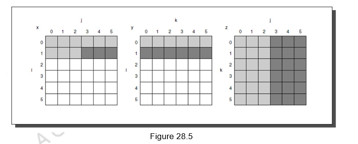
The number of capacity misses clearly depends on N and the size of the cache. If it can hold all three N by N matrices, then we don‘t have any problems, provided there are no cache conflicts. If the cache can hold one N by N matrix and one row of N, then at least the i-th row of y and the array z may stay in the cache. If we cannot accommodate even that in cache, then, misses may occur for both x and z. In the worst case, there would be 2N3 + N2 memory words accessed for N3 operations.
To ensure that the elements being accessed can fit in the cache, the original code is changed to compute on a submatrix of size B by B. Two inner loops now compute in steps of size B rather than the full length of x and z. B is called the blocking factor. (Assume x is initialized to zero.)
/\* After \*/
for (jj = 0; jj < N; jj = jj+B)
for (kk = 0; kk < N; kk = kk+B)
for (i = 0; i < N; i = i+1)
for (j = jj; j < min(jj+B,N); j = j+1)
{r = 0;
for (k = kk; k < min(kk+B,N); k = k + 1)
r = r + y\[i\]\[k\]\*z\[k\]\[j\];
x\[i\]\[j\] = x\[i\]\[j\] + r;
};
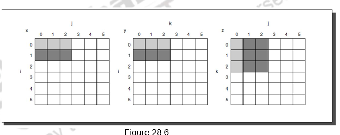
Figure 28.6 illustrates the accesses to the three arrays using blocking. Looking only at capacity misses, the total number of memory words accessed is 2N3/B + N2. This total is an improvement by about a factor of B. Hence, blocking exploits a combination of spatial and temporal locality, since y benefits from spatial locality and z benefits from temporal locality.
Although we have aimed at reducing cache misses, blocking can also be used to help register allocation. By taking a small blocking size such that the block can be held in registers, we can minimize the number of loads and stores in the program.
To summarize, we have defined the average memory access time in this module. The AMAT depends on the hit time, miss rate and miss penalty. Several optimizations exist to handle each of these factors. We discussed five different techniques for reducing the miss rates. They are:
- Larger block size
- Larger cache size
- Higher associativity
- Way prediction and pseudo associativity, and
- Compiler optimizations.
Web Links / Supporting Materials
- Computer Organization and Design – The Hardware / Software Interface, David A. Patterson and John L. Hennessy, 4th Edition, Morgan Kaufmann, Elsevier, 2009.
- Computer Architecture – A Quantitative Approach , John L. Hennessy and David A.Patterson, 5th Edition, Morgan Kaufmann, Elsevier, 2011.
- Computer Organization, Carl Hamacher, Zvonko Vranesic and Safwat Zaky, 5th.Edition, McGraw- Hill Higher Education, 2011.
Cache Optimizations III
The objectives of this module are to discuss the various factors that contribute to the average memory access time in a hierarchical memory system and discuss some of the techniques that can be adopted to improve the same.
Memory Access Time: In order to look at the performance of cache memories, we need to look at the average memory access time and the factors that will affect it. We know that the average memory access time (AMAT) is defined as
AMAT = htc + (1 – h) (tm + tc), where tc in the second term is normally ignored.
h : hit ratio of the cache, tc : cache access time, 1 – h : miss ratio of the cache and
tm : main memory access time
AMAT can be written as hit time + (miss rate x miss penalty). Reducing any of these factors reduces AMAT. The previous modules discussed some optimizations that are done to reduce the miss penalty and miss rate. We shall look at some more optimizations in this module. We shall discuss the techniques that can be used to reduce the miss penalty and miss rate via parallelism and also techniques that can be used to reduce the hit time. The following techniques will be discussed:
- Reducing the miss penalty or miss rate via parallelism
- Non-blocking caches
- Multi banked caches
- Hardware & compiler prefetching
- Reducing the time to hit in the cache
- Small and simple caches
- Avoiding address translation
- Pipelined cache access, and
- Trace caches
We shall examine each of these in detail. For the first category, where we try to reduce the miss penalty or miss rate through parallelism, there is an overlap of the execution of instructions with activities happening in the memory hierarchy.
Non-blocking caches: They are also called lock-up free caches. For processors that support out-of-order completion, the CPU need not stall on a cache miss. For example, the CPU continues fetching instructions from the instruction cache while waiting for the data cache to return the missing data. There is a possibility of having a hit under a miss. This “hit under miss” optimization reduces the effective miss penalty by being helpful during a miss instead of ignoring the requests of the CPU. We can also have even further optimizations like, a “hit under multiple miss” or “miss under miss” optimization. That is, even when there are multiple outstanding misses, we still allow the processor to access. However, all this significantly increases the complexity of the cache controller as there can be multiple outstanding memory accesses. Also, there will be difficulties with performance evaluation. A cache miss does not necessarily stall the CPU and there is a possibility of occurrence of more than one miss request to the same block. This has to be handled carefully. The hardware must check on misses to avoid incoherency problems and to save time.
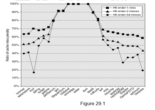
Figure 29.1 shows the average time in clock cycles for cache misses for an 8-KB data cache as the number of outstanding misses is varied. Floating-point programs benefit from the increasing complexity associated with multiple outstanding misses, while integer programs get almost all of the benefit from a simple hit-under-one-miss scheme.
Multi-banked caches: Instead of treating the cache as a single block of memory, we can organize the cache as a collection of independent banks to support simultaneous access. The same concept that was used to facilitate parallel access and increased bandwidth in main memories is used here also. The ARM Cortex A8 supports 1-4 banks for L2. The Intel i7 supports 4 banks for L1 and 8 banks for L2.
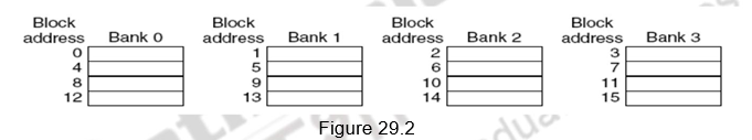
Banking supports simultaneous accesses only when the addresses are spread across multiple banks. The mapping of addresses to banks affects the behavior of the memory system. A simple way to spread the accesses across multiple blocks is sequential interleaving as shown in Figure 29.2. The figure shows four-way interleaved cache banks using block addressing. Block 0 is in bank 0, block 1 in bank1, block 2 in bank 2 and block 3 in bank 3. Now, block 4 is in bank 0, and so on. Blocks 0, 4, 8 and 12 are mapped to bank 0, blocks 1, 5, 9, 13 are mapped to block1, and so on. So, block number mod number of banks decides the bank number. Assuming 64 bytes per block, each of these addresses would be multiplied by 64 to get byte addressing. Multiple banks also help in reducing the power consumption.
Hardware based prefetching: One other technique to reduce miss penalty is to prefetch items before they are requested by the processor. Both instructions and data can be prefetched, either directly into the caches or into an external buffer that can be accessed faster than main memory. With respect to instruction prefetches, the processor typically fetches two blocks on a miss – the requested block and the next consecutive block. The requested block is placed in the instruction cache , while the prefetched block is placed into the instruction stream buffer. If the requested block is present in the instruction stream buffer, the original cache request is canceled, the block is read from the stream buffer, and the next prefetch request is issued. People have shown that there has been a lot of improvement seen with such prefetches.
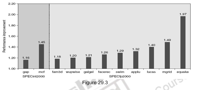
A similar approach can be applied to data accesses also. People have proved that a single data stream buffer caught about 25% of the misses from a 4-KB direct-mapped cache. Instead of having a single stream, there could be multiple stream buffers beyond the data cache, each prefetching at different addresses and this would increase the data hit rate. The UltraSPARC III uses such a prefetch scheme. A prefetch cache remembers the address used to prefetch the data. If a load hits in prefetch cache, the block is read from the prefetch cache, and the next prefetch request is issued. It calculates the “stride” of the next prefetched block using the difference between current address and the previous address. There can be up to eight simultaneous prefetches in UltraSPARC III. However, these prefetches should not interfere with demand based fetches. In that case, the performance will degrade. Figure 29.3 shows the performance improvement with prefetching in Pentium 4.
Compiler based prefetching: Just like hardware based prefetching, the compiler can also prefetch in order to reduce the miss rates and miss penalty. The compiler inserts prefetch instructions to request the data before they are needed. The two types of prefetch are:
- Register prefetch which loads the value into a register.
- Cache prefetch which loads data only into the cache and not the register.
Either of these can be faulting or non-faulting. That is, the address does or does not cause an exception for virtual address faults and protection violations. Non-faulting prefetches simply turn into no-ops if they would normally result in an exception. A normal load instruction could be considered a faulting register prefetch instruction. The most effective prefetch is “semantically invisible” to a program . It does not change the contents of registers and memory and it cannot cause virtual memory faults. Most processors today offer non-faulting cache prefetches. Like hardware-controlled prefetching, the goal is to overlap execution with the prefetching of data. Loops are the important targets, as they lend themselves to prefetch optimizations. If the miss penalty is small, the compiler just unrolls the loop once or twice and it schedules the prefetches with the execution. If the miss penalty is large, it uses software pipelining or unrolls many times to prefetch data for a future iteration. Issuing prefetch instructions incurs an instruction overhead, however, so care must be taken to ensure that such overheads do not exceed the benefits.
So far, we have looked at different techniques for reducing the miss penalty and miss rate via parallelism. Now, we shall discuss various techniques that are used to reduce the third component of AMAT, viz. hit time. This is about how to reduce time to access data that is in the cache. We shall look at techniques that are useful for quickly and efficiently finding out if data is in the cache, and if it is, getting that data out of the cache. Hit time is critical because it affects the clock rate of the processor . In many processors today, the cache access time limits the clock cycle rate, even for processors that take multiple clock cycles to access the cache. Hence, a fast hit time gains a lot of significance, beyond the average memory access time formula, because it helps everything.
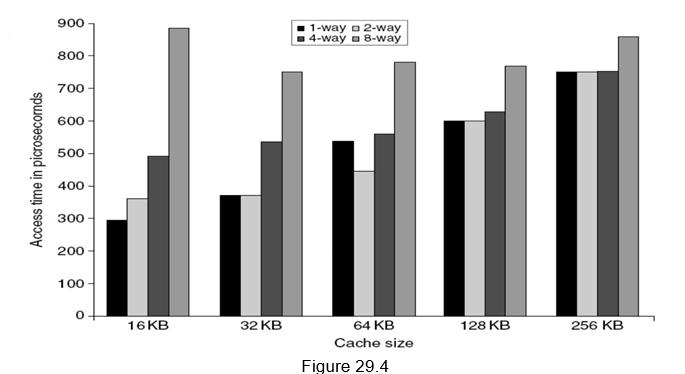
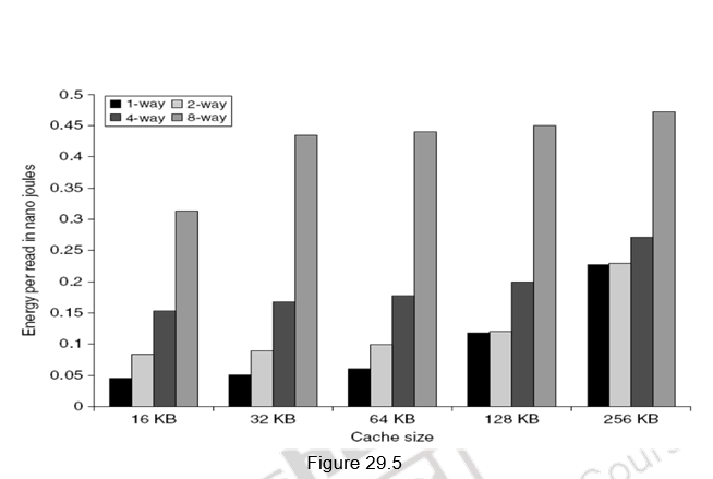
Small and simple first level caches: Small hardware is faster and hence a small and simple cache certainly helps the hit time. A smaller cache also enables it to be on chip and avoids the penalty associated with off chip caches. The c ritical timing path for accessing the cache includes addressing (indexing) tag memory, comparing tags and then getting the data. Direct-mapped caches can overlap the tag comparison and transmission of data. Since most of the data hits in the cache, saving a cycle on data access in the cache is a significant result. Lower associativity also reduces power because fewer cache lines are accessed. Figure 29.4 shows the effect of cache size and associativity on the access times. As the size/associativity increases, the access time increases. Figure 29.5 shows the effect of cache size and associativity on the energy per read. As the size/associativity increases, the energy per read increases.
Avoiding address translation during indexing of the caches: With the support for virtual memory, virtual addresses will have to first be translated to physical addresses and only then the indexing of the cache can happen. Going by the general guideline of making the common case fast, we can use virtual addresses for the cache, since hits are much more common than misses. Such caches are termed virtual caches, with physical cache used to identify the traditional cache that uses physical addresses.
As already pointed out, we have two tasks associated with accessing the cache – indexing the cache and the tag comparison. Thus, the issues are whether a virtual or physical address is used to index the cache and whether a virtual or physical index is used in the tag comparison. Full virtual addressing for both index and tags eliminates address translation time from a cache hit. But there are several reasons for not looking at such virtually addressed caches.
One reason is protection. Normally, the very essential page level protection is checked as part of the virtual to physical address translation. One solution when we use virtual caches is to copy the protection information from the TLB on a miss, add a field to hold it, and check it on every access to the virtually addressed cache. Another reason is that every time a process is switched, the virtual addresses refer to different physical addresses, requiring the cache to be flushed. This can be handled with a process-identifier tag (PID). If the operating system assigns these tags to processes, the PID distinguishes whether or not the data in the cache are for this program. A third reason why virtual caches are not more popular is that operating systems and user programs may use two different virtual addresses for the same physical address. These duplicate addresses, called synonyms or aliases, could result in two copies of the same data in a virtual cache. If one is modified, the other will have the wrong value. Hardware solutions to the synonym problem, called anti-aliasing, make sure that such problems do not occur. The Alpha 21264 uses a 64 KB instruction cache with an 8 KB page and two-way set associativity. Hence, the hardware must handle aliases involved with the 2 virtual address bits in both sets. It avoids aliases by simply checking all 8 possible locations on a miss–four entries per set, to be sure that none match the physical address of the data being fetched. If one is found, it is invalidated, so when the new data is loaded into the cache its physical address is guaranteed to be unique. Software can make this problem much easier by forcing aliases to share some address bits. Lastly, the final area of concern with virtual addresses is I/O. I/O typically uses physical addresses and thus would require mapping to virtual addresses to interact with a virtual cache.
One way to reap the benefits of both virtual and physical caches is to use part of the page offset, the part that is identical in both virtual and physical addresses to index the cache. When the cache is being indexed using the virtual address, the virtual part of the address is translated, and the tag match uses physical addresses. This is called a virtually indexed physically tagged cache. This alternative allows the cache read to begin immediately and yet the tag comparison is still with physical addresses. The limitation of this type of cache is that a direct-mapped cache cannot be larger than the page size.
Pipelining the cache access: The next technique that can be used to reduce the hit time, is to pipeline the cache access, so that the effective latency of a first level cache hit can be multiple clock cycles, giving fast cycle time and slow hits. For example, the pipeline for the Pentium takes one clock cycle to access the instruction cache, for the Pentium Pro through Pentium III it takes two clocks, and for the Pentium 4 to i7, it takes four clocks. This split increases the number of pipeline stages, leading to greater penalty on mis-predicted branches and more clock cycles between the issue of the load and the use of the data. This technique, in reality, increases the bandwidth of instructions rather than decreasing the actual latency of a cache hit. It also makes it easier to increase associativity.
Trace cache: The last technique that we discuss is the use of a trace cache. One of the main challenges in modern day processors is to find instruction level parallelism beyond four instructions per cycle, so that the integrated instruction unit is able to supply enough instructions every cycle without dependencies. One solution is called a trace cache. Instead of limiting the instructions in a static cache block to spatial locality, a trace cache finds a dynamic sequence of instructions including taken branches to load into a cache block. It is called a trace cache, because the cache blocks contain dynamic traces of the executed instructions as determined by the CPU, rather than containing static sequences of instructions as determined by memory. Hence, the branch prediction is folded into cache, and must be validated along with the addresses to have a valid fetch. The Intel Netburst microarchitecture, which is the foundation of the Pentium 4 and its successors, uses a trace cache.
Trace caches have much more complicated address mapping mechanisms, as the addresses are no longer aligned to power of 2 multiple of the word size. However, they have other benefits for utilization of the data portion of the instruction cache. With branches being very frequent, large blocks may be wasted in conventional caches. Space utilization is a real problem for processors like the AMD Athlon, whose 64 byte block would probably include16 to 24 80×86 instructions. The trend towards higher instruction issue makes the problem worse. Trace caches store instructions only from the branch entry point to the exit of the trace, thereby avoiding such under utilization. However, the downside of trace caches is that they store the same instructions multiple times in the instruction cache. Conditional branches making different choices result in the same instructions being part of separate traces, which each occupy space in the cache.
To summarize, we have defined the average memory access time in this module. The AMAT depends on the hit time, miss rate and miss penalty. Several optimizations exist to handle each of these factors . We discussed different techniques for reducing the miss penalty and miss rate via parallelism and for reducing the hit time . They are:
Ø Reducing the miss penalty or miss rate via parallelism
§ Non-blocking caches
§ Multi banked caches
§ Hardware & compiler prefetching
Ø Reducing the time to hit in the cache
§ Small and simple caches
§ Avoiding address translation
§ Pipelined cache access, and
§ Trace caches
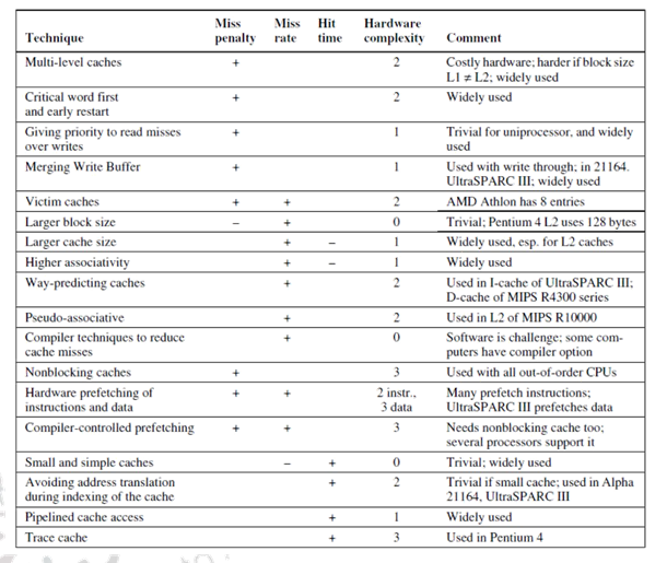
Figure 29.6
As a ready reckoner, Figure 29.6 gives a summary of all the cache optimization techniques that we have discussed in the past three modules.
Web Links / Supporting Materials
- Computer Organization and Design – The Hardware / Software Interface, David A. Patterson and John L. Hennessy, 4th Edition, Morgan Kaufmann, Elsevier, 2009.
- Computer Architecture – A Quantitative Approach , John L. Hennessy and David A.Patterson, 5th Edition, Morgan Kaufmann, Elsevier, 2011.
- Computer Organization, Carl Hamacher, Zvonko Vranesic and Safwat Zaky, 5th.Edition, McGraw- Hill Higher Education, 2011
Virtual Memory I
The objectives of this module are to discuss the concept of virtual memory and discuss the various implementations of virtual memory.
All of us are aware of the fact that our program needs to be available in main memory for the processor to execute it. Assume that your computer has something like 32 or 64 MB RAM available for the CPU to use. Unfortunately, that amount of RAM is not enough to run all of the programs that most users expect to run at once. For example, if you load the operating system, an e-mail program, a Web browser and word processor into RAM simultaneously, 32 MB is not enough to hold all of them. If there were no such thing as virtual memory, then you will not be able to run your programs, unless some program is closed. With virtual memory, we do not view the program as one single piece. We divide it into pieces, and only the one part that is currently being referenced by the processor need to be available in main memory. The entire program is available in the hard disk. As the copying between the hard disk and main memory happens automatically, you don’t even know it is happening, and it makes your computer feel like is has unlimited RAM space even though it only has 32 MB installed. Because hard disk space is so much cheaper than RAM chips, it also has a n economic benefit.
Techniques that automatically move program and data blocks into the physical main memory when they are required for execution are called virtual-memory techniques. Programs, and hence the processor, reference an instruction and data space that is independent of the available physical main memory space. The binary addresses that the processor issues for either instructions or data are called virtual or logical addresses. These addresses are translated into physical addresses by a combination of hardware and software components. If a virtual address refers to a part of the program or data space that is currently in the physical memory, then the contents of the appropriate location in the main memory are accessed immediately. On the other hand, if the referenced address is not in the main memory, its contents must be brought into a suitable location in the memory before they can be used. Therefore, an address used by a programmer will be called a virtual address, and the set of such addresses the address space. An address in main memory is called a location or physical address. The set of such locations is called the memory space, which consists of the actual main memory locations directly addressable for processing. As an example, consider a computer with a main-memory capacity of 32M words. Twenty-five bits are needed to specify a physical address in memory since 32 M = 225. Suppose that the computer has available auxiliary memory for storing 235, that is, 32G words. Thus, the auxiliary memory has a capacity for storing information equivalent to the capacity of 1024 main memories. Denoting the address space by N and the memory space by M, we then have for this example N = 32 Giga words and M = 32 Mega words.
The portion of the program that is shifted between main memory and secondary storage can be of fixed size (pages) or of variable size (segments). Virtual memory also permits a program’s memory to be physically noncontiguous , so that every portion can be allocated wherever space is available. This facilitates process relocation. Virtual memory, apart from overcoming the main memory size limitation, allows sharing of main memory among processes. Thus, the virtual memory model provides decoupling of addresses used by the program (virtual) and the memory addresses (physical). Therefore, the definition of virtual memory can be stated as, “ The conceptual separation of user logical memory from physical memory in order to have large virtual memory on a small physical memory”. It gives an illusion of infinite storage, though the memory size is limited to the size of the virtual address.
Even though the programs generate virtual addresses, these addresses cannot be used to access the physical memory. Therefore, the virtual to physical address translation has to be done. This is done by the memory management unit (MMU). The mapping is a dynamic operation, which means that every address is translated immediately as a word is referenced by the CPU. This concept is depicted diagrammatically in Figures 30.1 and 30.2. Figure 30.1 gives a general overview of the mapping between the logical addresses and physical addresses. Figure 30.2 shows how four different pages A, B, C and D are mapped. Note that, even though they are contiguous pages in the virtual space, they are not so in the physical space. Pages A, B and C are available in physical memory at non-contiguous locations, whereas, page D is not available in physical storage.
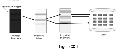
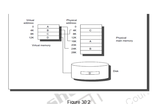
Address mapping using Paging: The address mapping is simplified if the informa tion in the address space and the memory space are each divided into groups of fixed size. The physical memory is broken down into groups of equal size called page frames and the logical memory is divided into pages of the same size. The programs are also considered to be split into pages. Pages commonly range from 2K to 16K bytes in length. They constitute the basic unit of information that is moved between the main memory and the disk whenever the translation mechanism determines that a move is required. Pages should not be too small, because the access time of a magnetic disk is much longer than the access time of the main memory. The reason for this is that it takes a considerable amount of time to locate the data on the disk, but once located, the data can be transferred at a rate of several megabytes per second. On the other hand, if pages are too large it is possible that a substantial portion of a page may not be used, yet this unnecessary data will occupy valuable space in the main memory. If you consider a computer with an address space of 1M and a memory space of 64K, and if you split each into groups of 2K words, you will obtain 29 (512) pages and thirty-two page frames. At any given time, up to thirty-two pages of address space may reside in main memory in anyone of the thirty-two blocks.
In order to do the mapping, the virtual address is represented by two numbers: a page number and an offset or line address within the page. In a computer with 2 p words per page, p bits are used to specify an offset and the remaining high-order bits of the virtual address specify the page number. In the example above, we considered a virtual address of 20 bits. Since each page consists of 211 = 2K words, the high order nine bits of the virtual address will specify one of the 512 pages and the low-order 11 bits give the offset within the page. Note that the line address in address space and memory space is the same; the only mapping required is from a page number to a block number.
The mapping information between the pages and the page frames is available in a page table. The page table consists of as many pages that a virtual address can support. The base address of the page table is stored in a register called the Page Table Base Register (PTBR). Each process can have one or more of its own page tables and the operating system switches from one page table to another on a context switch, by loading a different address into the PTBR. The page number, which is part of the virtual address, is used to index into the appropriate page table entry. The page table entry contains the physical page frame address, if the page is available in main memory. Otherwise, it specifies wherein secondary storage, the page is available. This generates a page fault and the operating system brings the requested page from secondary storage to main storage. Along with this address information, the page table entry also provides information about the privilege level associated with the page and the access rights of the page. This helps in p roviding protection to the page. The mapping process is indicated in Figure 30.3. Figure 30.4 shows a typical page table entry. The dirty or modified bit indicates whether the page was modified during the cache residency period.
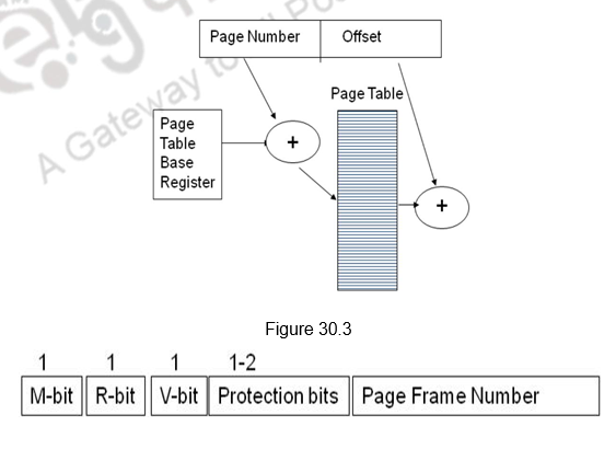 Figure 30.4
- M – indicates whether the page has been written (dirty)
- R – indicates whether the page has been referenced (useful for replacement)
- V – Valid bit
- Protection bits – indicate what operations are allowed on this page
- Page Frame Number says where in memory is the page
A virtual memory system is thus a combination of hardware and software tech-niques. The memory management software system handles all the software operations for the efficient utilization of memory space. It must decide the answers to the usual four questions in a hierarchical memory system:
- Q1: Where can a block be placed in the upper level?
- Q2: How is a block found if it is in the upper level?
- Q3: Which block should be replaced on a miss?
- Q4: What happens on a write?
The hardware mapping mechanism and the memory management software together constitute the architecture of a virtual memory and answer all these questions .
When a program starts execution, one or more pages are transferred into main memory and the page table is set to indicate their position. Thus, the page table entries help in identifying a page. The program is executed from main memory until it attempts to reference a page that is still in auxiliary memory. This condition is called a page fault. When a page fault occurs, the execution of the present program is suspended until the required page is brought into main memory. Since loading a page from auxiliary memory to main memory is basically an I/O operation, the operating system assigns this task to the I/O processor. In the meantime, control is transferred to the next program in memory that is waiting to be processed in the CPU. Later, when the memory block has been assigned and the transfer completed, the original program can resume its operation. It should be noted that it is always a write back policy that is adopted, because of the long access times associated with the disk access. Also, when a page fault is serviced, the memory may already be full. In this case, as we discussed for caches, a replacement has to be done. The replacement policies are again FIFO and LRU. The FIFO replacement policy has the advantage of being easy to implement. !t has the disadvantage that under certain circumstances pages are removed and loaded from memory too frequently. The LRU policy is more difficult to implement but has been more attractive on the assumption that the least recently used page is a better candidate for removal than the least recently loaded page as in FIFO. The LRU algorithm can be implemented by associating a counter with every page that is in main memory. When a page is referenced, its associated counter is set to zero. At fixed intervals of time, the counters associated with all pages presently in memory are incremented by 1. The least recently used page is the page with the highest count. The counters are often called aging registers, as their count indicates their age, that is, how long ago their associated pages have been referenced.
Drawback of Virtual memory: So far we have assumed that the page tables are stored in memory. Since, the page table information is used by the MMU, which does the virtual to physical address translation, for every read and write access, every memory access by a program can take at least twice as long: one memory access to obtain the physical address and a second access to get the data. So, ideally, the page table should be situated within the MMU. Unfortunately, the page table may be rather large, and since the MMU is normally implemented as part of the processor chip, it is impossible to include a complete page table on this chip. Therefore, the page table is kept in the main memory. However, a copy of a small portion of the page table can be accommodated within the MMU. This portion consists of the page table entries that correspond to the most recently accessed pages. A small cache, usually called the Translation Lookaside Buffer (TLB) is incorporated into the MMU for this purpose. The TLB stores the most recent logical to physical address translations. The operation of the TLB with respect to the page table in the main memory is essentially the same as the operation we have discussed in conjunction with the cache memory. Figure 30.5 shows a possible organization of a TLB where the associative mapping technique is used. Set-associative mapped TLBs are also found in commercial products. The TLB gives information about the validity of the page, status of whether it is available in physical memory, protection information, etc. apart from the physical address.
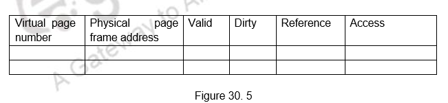
An essential requirement is that the contents of the TLB be coherent with the contents of page tables in the memory. When the operating system changes the contents of page tables, it must simultaneously invalidate the corresponding entries in the TLB. The valid bit in the TLB is provided for this purpose. When an entry is invalidated, the TLB will acquire the new information as part of the MMU’s normal response to access misses.
With the introduction of the TLB, the address translation proceeds as follows. Given a virtual address, the MMU looks in the TLB for the referenced page. If the page table entry for this page is found in the TLB, the physical address is obtained immediately. If there is a miss in the TLB, then the required entry is obtained from the page table in the main memory and the TLB is updated.
Recall that the caches need a physical address, unless we use virtual caches. As discussed with respect to cache optimizations, machines with TLBs go one step further to reduce the number of cycles/cache access. They overlap the cache access with the TLB access. That is, the high order bits of the virtual address are used to look in the TLB while the low order bits are used as index into the cache. The flow is as shown below.
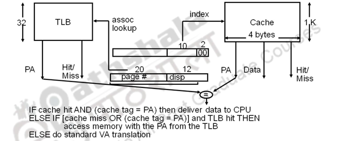
The overlapped access only works as long as the address bits used to index into the cache do not change as the result of VA translation. This usually limits things to small caches, large page sizes, or high n-way set associative caches if you want a large cache.
Finally, we shall have a word on the types of misses that can occur in a hierarchical memory system. This is again similar to the misses that we have already discussed with respect to cache memory. The misses are summarized as follows:
• Compulsory Misses:
– Pages that have never been paged into memory before
– How might we remove these misses?
• Prefetching: loading them into memory before needed
• Need to predict future somehow!
• Capacity Misses:
– Not enough memory. Must somehow increase size.
– Can we do this?
- One option: Increase amount of DRAM
- Another option: If multiple processes in memory: adjust percentage of memory allocated to each one!
- Conflict Misses:
– Technically, conflict misses don’t exist in virtual memory, since it is a “fully-associative” cache
- Policy Misses:
– Caused when pages were in memory, but kicked out prematurely because of the replacement policy
– How to fix? Better replacement policy
To summarize, we have looked at the need for the concept of virtual memory. Virtual memory is a concept implemented using hardware and software. The restriction placed on the program si ze is not based on the RAM size, but based on the virtual memory size. There are three different ways of implementing virtual memory. The MMU does the logical to physical address translation. Paging uses fixed size pages to move between main memory and secondary storage. Paging uses page tables to map the logical addresses to physical addresses. Thus, virtual memory helps in dynamic allocation of the required data, sharing of data and providing protection. The TLB is used to store the most recent logical to physical address translations.
Virtual Memory II
The objectives of this module are to discuss the other implementations of virtual memory, viz, segmentation and segmented paging and compare and contrast the various implementations of virtual memory. The concept of virtual machines will be introduced. Also, the various techniques used for improving the main memory access time will be discussed.
Address Mapping Using Segments: The previous module discussed in detail about the virtual memory management system, where the main memory and the programs were divided into pages of equal size. But, the fixed page size causes certain difficulties with respect to program size and the logical structure of programs. It is more convenient to divide programs and data into logical parts called segments. A segment is a set of logically related instructions or data elements associated with a given name. Segments may be generated by the programmer or by the operating system. Examples of seg-ments are a subroutine, an array of data, a table of symbols, or a user’s program. As in paging, the address generated by a segmented program is called a logical address. This is similar to a virtual address except that logical address space is associated with variable-length segments rather than fixed -length pages. The logical address consists of the segment number and the offset. The segment number is mapped to a physical address using segment descriptor tables. These tables do the same function as the page tables in paging. Because the segments can vary is size, a bounds check is also needed to make sure that the offset is within the segment. The function of the memory management unit is to map logical addresses into physical addresses similar to the virtual memory mapping concept. The segmentation concept is illustrated in Figure 31.1.
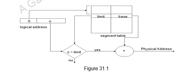
In addition to relocation information, each segment descriptor entry has protection information associated with it. Segmentation offers the advantage of sharing commonly used data and programs. Shared programs are placed in a unique segment in each user’s logical address space so that a single physical copy can be shared.
Segments cannot be broken further and the entire segment has to be either in memory or on disk. The variable sizes of the segments leads to external fragmentation in memory, whereas, in paging we have only internal fragmentation, where the last page alone may not be completely filled. When it comes to bringing in a new segment into main memory also, we have more complications. In the case of paging, all the blocks are of the same size. Therefore, any block can replace any block. However, as segments are of varying sizes, the operating system has to identify a segment large enough to accommodate the incoming segment. This is done with the following techniques:
- First fit – The first segment that is big enough to accommodate the incoming segment is chosen.
- Best fit – The best fitting segment, that is, the one leaving the least amount of free space is chosen. For example, if the segment size is 4K, and the available segments are of sizes 5K and 8K, the 5K segment will be chosen.
- Worst fit – The one that is the worst fit, leaving the maximum space will be chosen. In the previous example, the segment of size 8K will be chosen.
Note that the TLB is used in the case of segmentation also to speed up the memory access.
Address Mapping Using Segmented Paging: It is also possible to have a third memory management technique called segmented paging. As the name suggests, this is a combination of both segmentation and paging. It was already mentioned that the property of logical space is that it uses variable-length segments. The length of each segment is allowed to grow and contract according to the needs of the program being executed. One way of specifying the length of a segment is by associating with it a number of equal-sized pages. To see how this is done, consider the logical address shown in Figure 31.2. The logical address is partitioned into three fields. The segment field specifies a segment number. The page field specifies the page within the segment and the word field gives the specific word within the page. A page field of k bits can specify up to 2k pages. A segment number may be associated with just one page or with as many as 2k pages. Thus the length of a segment would vary according to the number of pages that are assigned to it.
The mapping of the logical address into a physical address is done by means of two tables. The segment number of the logical address specifies the address for the segment table. The entry in the segment table is a pointer address for a page table base. This new address is often referred to as a linear address . The page table base is added to the page number given in the logical address. The sum produces a pointer address to an entry in the page table. The value found in the page table provides the block number in physical memory. The concatenation of the block field with the word field produces the final physical mapped address.
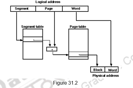
We thus use pages to describe components of the segments . This makes segments easy to manage and we can swap memory between segments . We need to allocate page table entries only for those pieces of the segments that have themselves been allocated. Segments that are shared can be represented with shared page tables. The two mapping tables may be stored in main memory. Therefore, a memory reference from the CPU will require three accesses to memory – one from the segment table, one from the page table, and the third from main memory. This would slow the system even more. To avoid this speed penalty, the TLB is used in this case also.
Memory Management System: In a multiprogramming environment where many programs reside in memory, it becomes necessary to move programs and data around the memory, to vary the amount of memory in use by a given program, and to prevent a program from changing other programs. The demands on computer memory brought about by multiprogramming have created the need for a memory management system. A memory management system is a collection of hardware and software procedures for managing the various programs residing in memory. The memory management software is part of an overall operating system available in many computers. The hardware includes the page tables, segment tables and TLBs in the MMU as pointed out in the previous section. Putting everything together, we can say that the basic components of a memory management system are:
1. A facility for dynamic storage relocation that maps logical memory references into physical memory addresses
2. A provision for sharing common programs stored in memory by differ ent users
3. Protection of information against unauthorized access between users and preventing users from changing operating system functions.
The first function of dynamic storage relocation is what we discussed in the previous section.
The sharing of common programs is an integral part of a multiprogramming system. For example, several users wishing to compile their C programs should be able to share a single copy of the compiler rather than each user having a separate copy in memory. Other system programs residing in memory are also shared by all users in a multiprogramming system without having to produce multiple copies.
The third issue in multiprogramming is protecting one program from unwanted interaction with another. An example of unwanted interaction is one user’s unauthorized copying of another user’s program. Another aspect of protection is concerned with preventing the occasional user from performing operating system functions and thereby interrupting the orderly sequence of operations in a computer installation. The secrecy of certain programs must be kept from unauthorized personnel to prevent abuses in the confidential activities of an organization. This feature is again supported in virtual memory by providing support for the addition of protection and access rights information in every page/segment. The following features are supported by the architecture in order to provide protection:
- Provide at least two modes, indicating whether the running process is a user process or an operating system process, called a kernel process or a supervisor process.
- Provide a portion of the processor state that a user process can use but not modify. This state includes an user/supervisor mode bit(s), an exception enable/disable bit, and memory protection information. Users are prevented from writing this state because the operating system cannot control user processes if users can give themselves supervisor privileges, disable exceptions, or change memory protection.
- Provide mechanisms whereby the processor can go from user mode to supervisor mode and vice versa. The first direction is typically accomplished by a system call, implemented as a special instruction that transfers control to a dedicated location in supervisor code space. The PC is saved from the point of the system call, and the processor is placed in supervisor mode. The return to user mode is like a subroutine return that restores the previous user/supervisor mode.
- Provide mechanisms to limit memory accesses to protect the memory state of a process without having to swap the process to disk on a context switch.
Thus, the above discussion clearly shows that we can enforce protection through the operating system with the support of architecture. However, the operating systems consist of tens of millions of lines of code and there are quite a lot of bugs here. Flaws in the OS have led to vulnerabilities that are routinely exploited. This problem, and the possibility that not enforcing protection could be much more costly than in the past, has led some to look for a protection model with a much smaller code base than the full OS, such as Virtual Machines.
Virtual Machines and Protection: Although virtual machines were not very popular in single-user computers, they have recently gained popularity due to the following reasons:
- the increasing importance of isolation and security in modern systems
- the failures in security and reliability of standard operating systems
- the sharing of a single computer among many unrelated users, and
- the dramatic increases in raw speed of processors, which makes the overhead of VMs more acceptable.
VMs provide a complete system-level environment at the binary instruction set architecture (ISA) level. They present the illusion that the users of a VM have an entire computer to themselves, including a copy of the operating system. A single computer runs multiple VMs and can support a number of different operating systems. On a conventional platform, a single OS “owns” all the hardware resources, but with a VM, multiple operating systems share the hardware resources. The software that supports VMs is called a virtual machine monitor (VMM) or hypervisor; the VMM is the heart of Virtual Machine technology. The underlying hardware platform is called the host, and its resources are shared among the guest VMs. The VMM determines how to map virtual resources to physical resources. A physical resource may be time -shared, partitioned, or even emulated in software. The VMM is much smaller than a traditional OS. Each guest OS maintains its own set of page tables. The VMM adds a level of memory between physical and virtual memory called “real memory” and the VMM maintains shadow page table that maps guest virtual addresses to physical addresses.
Improving the access times of main memory: Last of all, we shall look at various techniques that are used to improve the performance of main memory. Figure 31.3 shows various methods used to increase the bandwidth of main memory. The first method is a simple one where the CPU, cache, bus and memory have the same width, say 32 or 64 bits. The second one shows a wide memory organization, where the CPU/Mux width is 1 word. However, the Mux/Cache, bus and memory width are N words. The Alpha processor uses 64 bits & 256 bits and the UtraSPARC uses 64 bits and 512 bits. The third organization shows an interleaved organization, where the CPU, cache and bus have a width of 1 word, but the memory has N Modules (say, 4 Modules); for example, word interleaved. First-level caches are often organized with a physical width of 1 word because most CPU accesses are of that size. There is additional cost involved in the wider connection between the CPU and memory, typically called a memory bus. This may help for the second-level caches, since the multiplexing can be between the first and second level caches, and not on the critical path.
Memory chips can be organized in banks to read or write multiple words at a time rather than a single word. The mapping of the addresses to banks affects the behavior of the memory system. This mapping is called the Interleaving Factor. Interleaving Memory normally means banks of memory that are word interleaved. It is used to optimize sequential memory accesses. A cache read miss is an ideal match to word-interleaved memory, because the words in a block are read sequentially. Write-back caches make writes as well as reads sequential, getting even more efficiency from word-interleaved memory. However, the disadvantages are the shrinking number of chips and the difficulty of main memory expansion.
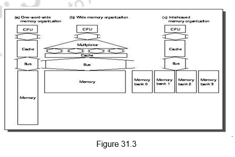
We can also look at independent memory banks, where each bank needs separate address lines and possibly a separate data bus. This is particularly useful with nonblocking caches that allow the CPU to proceed beyond a cache miss, potentially allowing multiple cache misses to be serviced simultaneously. Otherwise, the multiple reads will be serviced by a single memory port and will get only a small benefit of overlapping access with transmission. Normally, independent of memory technology, higher bandwidth is made available using memory banks, by making memory and its bus wider, or doing both.
Summary
- Techniques that automatically move program-and data blocks into the physical main memory when they are required for execution are called virtual-memory techniques.
- Virtual memory is a concept implemented using hardware and software.
- The restriction placed on the program size is not based on the RAM size, but based on the virtual memory size.
- There are three different ways of implementing virtual memory.
- The MMU does the logical to physical address translation.
- Paging uses fixed size pages to move between main memory and secondary storage.
- Paging uses page tables to map the logical addresses to physical addresses.
- Segmentation uses varying sized segments.
- Segmented paging combines paging and segmentation.
- TLB is used to store the most recent logical to physical address translations.
- Virtual memory helps in separating the user and supervisor programs and also one user’s program from another.
- Virtual machines also help in providing isolation and protection.
- Main memory bandwidth can be increased by different techniques .
- We can use a wider main memory or an interleaved main memory to increase the bandwidth.
Web Links / Supporting Materials
- Computer Organization and Design – The Hardware / Software Interface, David A. Patterson and John L. Hennessy, 4th Edition, Morgan Kaufmann, Elsevier, 2009.
- Computer Architecture – A Quantitative Approach , John L. Hennessy and David A.Patterson, 5th Edition, Morgan Kaufmann, Elsevier, 2011.
- Computer Organization, Carl Hamacher, Zvonko Vranesic and Safwat Zaky, 5th.Edition, McGraw- Hill Higher Education, 2011.