Execution of a Complete Instruction
Execution of a Complete Instruction – Datapath Implementation
The objectives of this module are to discuss how an instruction gets executed in a processor and the datapath implementation, using the MIPS architecture as a case study.
The characteristics of the MIPS architecture is first of all summarized below:
• 32bit byte addresses aligned – MIPS uses 32 bi addresses that are aligned.
• Load/store only displacement addressing – It is a load/store ISA or register/register ISA, where only the load and store instructions use memory operands. All other instructions use only register operands. The addressing mode used for the memory operands is displacement addressing, where a displacement has to be added to the base register contents to get the effective address.
• Standard data types – The ISA supports all standard data types.
• 32 GPRs – There are 32 general purpose registers, with register R0 always having 0.
• 32 FPRs – There are 32 floating point registers.
• FP status register – There ia floating point status register.
• No Condition Codes – MIPS architecture does not support condition codes.
• Addressing Modes – The addressing modes supported are Immediate, Displacement and Register Mode (used only for ALU)
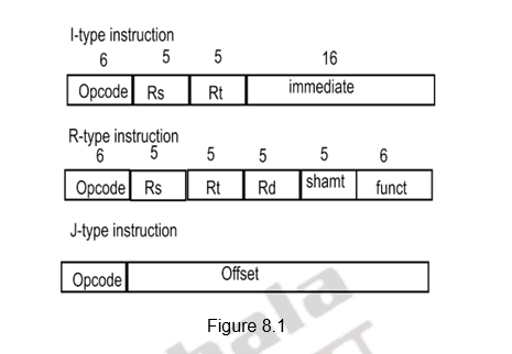
3 fixed length formats – There are 3 32-bit instruction formats that are supported. They are shown below in Figure 8.1.
We will examine the MIPS implementation for a simple subset that shows most aspects of implementation. The instructions considered are:
- The memory-reference instructions load word (lw) and store word (sw)
- The arithmetic-logical instructions add, sub, and, or, and slt
- The instructions branch equal (beq) and jump (j) to be considered in the end.
This subset does not include all the integer instructions (for example, shift, multiply, and divide are missing), nor does it include any floating-point instructions. However, the key principles used in creating a datapath and designing the control will be illustrated. The implementation of the remaining instructions is similar. The key design principles that we have looked at earlier can be illustrated by looking at the implementation, such as the common guidelines, ‘Make the common case fast’ and ‘Simplicity favors regularity’. In addition, most concepts used to implement the MIPS subset are the same basic ideas that are used to construct a broad spectrum of computers, from high-performance servers to general-purpose microprocessors to embedded processors.
When we look at the instruction cycle of any processor, it should involve the following operations:
- Fetch instruction from memory
- Decode the instruction
- Fetch the operands
- Execute the instruction
- Write the result
We shall look at each of these steps in detail for the subset of instructions. Much of what needs to be done to implement these instructions is the same, independent of the exact class of instruction. For every instruction, the first two steps of instruction fetch and decode are identical:
- Send the program counter (PC) to the program memory that contains the code and fetch the instruction
- Read one or two registers, using the register specifier fields in the instruction. For the load word instruction, we need to read only one register, but most other instructions require that we read two registers. Since MIPS uses a fixed length format with the register specifiers in the same place, the registers can be read, irrespective of the instruction.
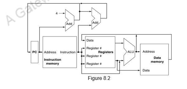
After these two steps, the actions required to complete the instruction depend on the type of instruction. For each of the three instruction classes, arithmetic/logical, memory-reference and branches, the actions are mostly the same. Even across different instruction classes there are some similarities. For example, all instruction classes, except jump, use the arithmetic and logical unit, ALU after reading the registers. The load / store memory-reference instructions use the ALU for effective address calculation, the arithmetic and logical instructions for the operation execution, and branches for condition evaluation, which is comparison here. As we can see, the simplicity and regularity of the instruction set simplifies the implementation by making the execution of many of the instruction classes similar. After using the ALU, the actions required to complete various instruction classes differ. A memory-reference instruction will need to access the memory. For a load instruction, a memory read has to be performed. For a store instruction, a memory write has to be performed. An arithmetic/logical instruction must write the data from the ALU back into a register. A load instruction also has to write the data fetched form memory to a register. Lastly, for a branch instruction, we may need to change the next instruction address based on the comparison. If the condition of comparison fails, the PC should be incremented by 4 to get the address of the next instruction. If the condition is true, the new address will have to updated in the PC. Figure 8.2 below gives an overview of the CPU.
However, wherever we have two possibilities of inputs, we cannot join wires together.
We have to use multiplexers as indicated below in Figure 8.3.
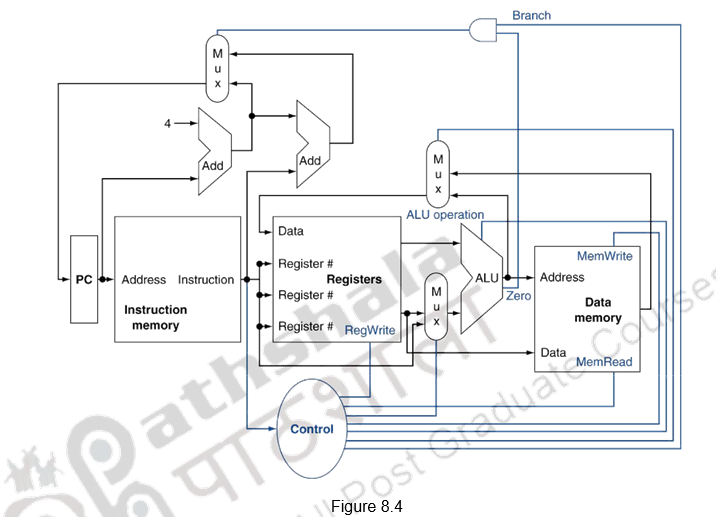
We also need to include the necessary control signals. Figure 8.4 below shows the datapath, as well as the control lines for the major functional units. The control unit takes in the instruction as an input and determines how to set the control lines for the functional units and two of the multiplexors. The third multiplexor, which determines whether PC + 4 or the branch destination address is written into the PC, is set based on the zero output of the ALU, which is used to perform the comparison of a branch on equal instruction. The regularity and simplicity of the MIPS instruction set means that a simple decoding process can be used to determine how to set the control lines.
Just to give a brief section on the logic design basics, all of you know that information is encoded in binary as low voltage = 0, high voltage = 1 and there is one wire per bit. Multi-bit data are encoded on multi-wire buses. The combinational elements operate on data and the output is a function of input. In the case of state (sequential) elements, they store information and the output is a function of both inputs and the stored data, that is, the previous inputs. Examples of combinational elements are AND-gates, XOR-gates, etc. An example of a sequential element is a register that stores data in a circuit. It uses a clock signal to determine when to update the stored value and is edge-triggered.
Now, we shall discuss the implementation of the datapath. The datapath comprises of the elements that process data and addresses in the CPU – Registers, ALUs, mux’s, memories, etc. We will build a MIPS datapath incrementally. We shall construct the basic model and keep refining it.
The portion of the CPU that carries out the instruction fetch operation is given in Figure 8.5.
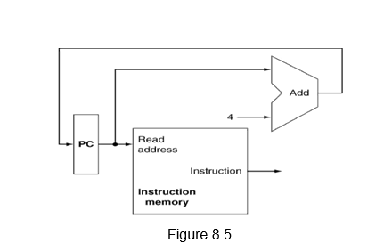
As mentioned earlier, The PC is used to address the instruction memory to fetch the instruction. At the same time, the PC value is also fed to the adder unit and added with 4, so that PC+4, which is the address of the next instruction in MIPS is written into the PC, thus making it ready for the next instruction fetch.

The next step is instruction decoding and operand fetch. In the case of MIPS, decoding is done and at the same time, the register file is read. The processor’s 32 general-purpose registers are stored in a structure called a register file. A register file is a collection of registers in which any register can be read or written by specifying the number of the register in the file.
The R-format instructions have three register operands and we will need to read two data words from the register file and write one data word into the register file for each instruction. For each data word to be read from the registers, we need an input to the register file that specifies the register number to be read and an output from the register file that will carry the value that has been read from the registers. To write a data word, we will need two inputs- one to specify the register number to be written and one to supply the data to be written into the register. The 5-bit register specifiers indicate one of the 32 registers to be used.
The register file always outputs the contents of whatever register numbers are on the Read register inputs. Writes, however, are controlled by the write control signal, which must be asserted for a write to occur at the clock edge. Thus, we need a total of four inputs (three for register numbers and one for data) and two outputs (both for data), as shown in Figure 8.6. The register number inputs are 5 bits wide to specify one of 32 registers, whereas the data input and two data output buses are each 32 bits wide.
After the two register contents are read, the next step is to pass on these two data to the ALU and perform the required operation, as decided by the control unit and the control signals. It might be an add, subtract or any other type of operation, depending on the opcode. Thus the ALU takes two 32-bit inputs and produces a 32-bit result, as well as a 1-bit signal if the result is 0. The control signals will be discussed in the next module. For now, we wil assume that the appropriate control signals are somehow generated.
The same arithmetic or logical operation with an immediate operand and a register operand, uses the I-type of instruction format. Here, Rs forms one of the source operands and the immediate component forms the second operand. These two will have to be fed to the ALU. Before that, the 16-bit immediate operand is sign extended to form a 32-bit operand. This sign extension is done by the sign extension unit.
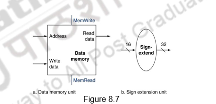
We shall next consider the MIPS load word and store word instructions, which have the general form lw t2) or sw t2). These instructions compute a memory address by adding the base register, which is t1. If the instruction is a load, the value read from memory must be written into the register file in the specified register, which is $t1. Thus, we will need both the register file and the ALU. In addition, the sign extension unit will sign extend the 16-bit offset field in the instruction to a 32-bit signed value. The next operation for the load and store operations is the data memory access. The data memory unit has to be read for a load instruction and the data memory must be written for store instructions; hence, it has both read and write control signals, an address input, as well as an input for the data to be written into memory. Figure 8.7 above illustrates all this.
The branch on equal instruction has three operands, two registers that are compared for equality, and a 16-bit offset used to compute the branch target address, relative to the branch instruction address. Its form is beq t2, offset. To implement this instruction, we must compute the branch target address by adding the sign-extended offset field of the instruction to the PC. The instruction set architecture specifies that the base for the branch address calculation is the address of the instruction following the branch. Since we have already computed PC + 4, the address of the next instruction, in the instruction fetch datapath, it is easy to use this value as the base for computing the branch target address. Also, since the word boundaries have the 2 LSBs as zeros and branch target addresses must start at word boundaries, the offset field is shifted left 2 bits. In addition to computing the branch target address, we must also determine whether the next instruction is the instruction that follows sequentially or the instruction at the branch target address. This depends on the condition being evaluated. When the condition is true (i.e., the operands are equal), the branch target address becomes the new PC, and we say that the branch is taken. If the operands are not equal, the incremented PC should replace the current PC (just as for any other normal instruction); in this case, we say that the branch is not taken.
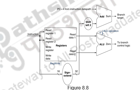
Thus, the branch datapath must do two operations: compute the branch target address and compare the register contents. This is illustrated in Figure 8.8. To compute the branch target address, the branch datapath includes a sign extension unit and an adder. To perform the compare, we need to use the register file to supply the two register operands. Since the ALU provides an output signal that indicates whether the result was 0, we can send the two register operands to the ALU with the control set to do a subtract. If the Zero signal out of the ALU unit is asserted, we know that the two values are equal. Although the Zero output always signals if the result is 0, we will be using it only to implement the equal test of branches. Later, we will show exactly how to connect the control signals of the ALU for use in the datapath.
Now, that we have examined the datapath components needed for the individual instruction classes, we can combine them into a single datapath and add the control to complete the implementation. The combined datapath is shown Figure 8.9 below.
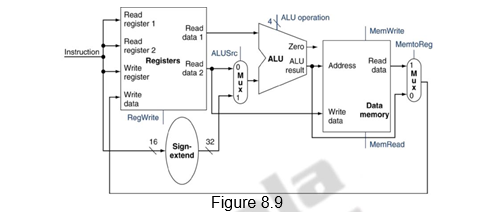
The simplest datapath might attempt to execute all instructions in one clock cycle. This means that no datapath resource can be used more than once per instruction, so any element needed more than once must be duplicated. We therefore need a memory for instructions separate from one for data. Although some of the functional units will need to be duplicated, many of the elements can be shared by different instruction flows. To share a datapath element between two different instruction classes, we may need to allow multiple connections to the input of an element, using a multiplexor and control signal to select among the multiple inputs. While adding multiplexors, we should note that though the operations of arithmetic/logical ( R-type) instructions and the memory related instructions datapath are quite similar, there are certain key differences.
- The R-type instructions use two register operands coming from the register file. The memory instructions also use the ALU to do the address calculation, but the second input is the sign-extended 16-bit offset field from the instruction.
- The value stored into a destination register comes from the ALU for an R-type instruction, whereas, the data comes from memory for a load.
To create a datapath with a common register file and ALU, we must support two different sources for the second ALU input, as well as two different sources for the data stored into the register file. Thus, one multiplexor needs to be placed at the ALU input and another at the data input to the register file, as shown in Figure 8.10.
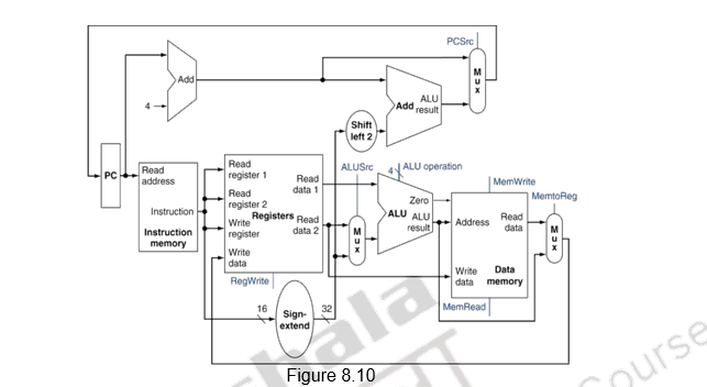
We have discussed the individual instructions – arithmetic/logical, memory related and branch. Now we can combine all the pieces to make a simple datapath for the MIPS architecture by adding the datapath for instruction fetch, the datapath from R-type and memory instructions and the datapath for branches. Figure below shows the datapath we obtain by combining the separate pieces. The branch instruction uses the main ALU for comparison of the register operands, so we must keep the adder shown earlier for computing the branch target address. An additional multiplexor is required to select either the sequentially following instruction address, PC + 4, or the branch target address to be written into the PC.
To summarize, we have looked at the steps in the execution of a complete instruction with MIPS as a case study. We have incrementally constructed the datapath for the Arithmetic/logical instructions, Load/Store instructions and the Branch instruction. The implementation of the jump instruction to the datapath and the control path implementation will be discussed in the next module.
Web Links / Supporting Materials
- Computer Organization and Design – The Hardware / Software Interface, David A. Patterson and John L. Hennessy, 4th.Edition, Morgan Kaufmann, Elsevier, 2009.
- Computer Organization, Carl Hamacher, Zvonko Vranesic and Safwat Zaky, 5th.Edition, McGraw- Hill Higher Education, 2011.
Execution of a Complete Instruction – Control Flow
The objectives of this module are to discuss how the control flow is implemented when an instruction gets executed in a processor, using the MIPS architecture as a case study and discuss the basics of microprogrammed control.
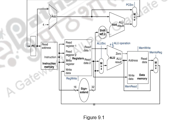
The control unit must be capable of taking inputs about the instruction and generate all the control signals necessary for executing that instruction, for eg. the write signal for each state element, the selector control signal for each multiplexor, the ALU control signals, etc. Figure 9.1 below shows the complete data path implementation for the MIPS architecture along with an indication of the various control signals required.
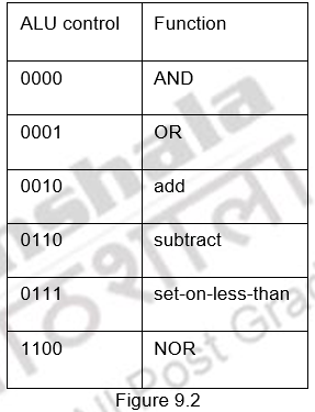
We shall first of all look at the ALU control. The implementation discussed here is specifically for the MIPS architecture and for the subset of instructions pointed out earlier. You just need to get the concepts from this discussion. The ALU uses 4 bits for control. Out of the 16 possible combinations, only 6 are used for the subset under consideration. This is indicated in Figure 9.2. Depending on the type of instruction class, the ALU will need to perform one of the first five functions. (NOR is needed for other parts of the MIPS instruction set not discussed here.) For the load word and store word instructions, we use the ALU to compute the memory address. This is done by addition. For the R-type instructions, the ALU needs to perform one of the five actions (AND, OR, subtract, add, or set on less than), depending on the value of the 6-bit funct (or function) field in the low-order bits of the instruction (refer to the instruction formats). For a branch on equal instruction, the ALU must perform a subtraction, for comparison.
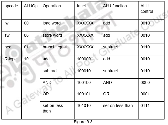
We can generate the 4-bit ALU control input using a small control unit that takes as inputs the function field of the instruction and a 2-bit control field, which we call ALUOp. ALUOp indicates whether the operation to be performed should be add (00) for loads and stores, subtract (01) for beq, or determined by the operation encoded in the funct field (10). The output of the ALU control unit is a 4-bit signal that directly controls the ALU by generating one of the 4-bit combinations shown previously. In Figure 9.3, we show how to set the ALU control inputs based on the 2-bit ALUOp control and the 6-bit function code. The opcode, listed in the first column, determines the setting of the ALUOp bits. When the ALUOp code is 00 or 01, the desired ALU action does not depend on the function code field and this is indicated as don’t cares, and the funct field is shown as XXXXXX. When the ALUOp value is 10, then the function code is used to set the ALU control input.
For completeness, the relationship between the ALUOp bits and the instruction opcode is also shown. Later on we will see how the ALUOp bits are generated from the main control unit. This style of using multiple levels of decoding—that is, the main control unit generates the ALUOp bits, which then are used as input to the ALU control that generates the actual signals to control the ALU unit—is a common implementation technique. Using multiple levels of control can reduce the size of the main control unit. Using several smaller control units may also potentially increase the speed of the control unit. Such optimizations are important, since the control unit is often performance-critical.
There are several different ways to implement the mapping from the 2-bit ALUOp field and the 6-bit funct field to the three ALU operation control bits. Because only a small number of the 64 possible values of the function field are of interest and the function field is used only when the ALUOp bits equal 10, we can use a small piece of logic that recognizes the subset of possible values and causes the correct setting of the ALU control bits.
Now, we shall consider the design of the main control unit. For this, we need to remember the following details about the instruction formats of the MIPS ISA. All these details are indicated in Figure 9.4.
- For all the formats, the opcode field is always contained in bits 31:26 – Op[5:0]
- The two registers to be read are always specified by the Rs and Rt fields, at positions 25:21 and 20:16. This is true for the R-type instructions, branch on equal, and for store
- The base register for the load and store instructions is always in bit positions 25:21 (Rs)
- The destination register is in one of two places. For a load it is in bit positions 20:16 (Rt), while for an R-type instruction it is in bit positions 15:11 (Rd). To select one of these two registers, a multiplexor is needed.
- The 16-bit offset for branch equal, load, and store is always in positions 15:0.
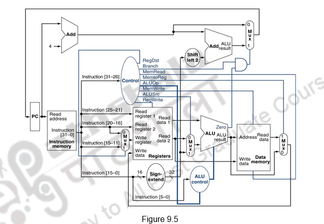
To the simple datapath already shown, we shall add all the required control signals. Figure 9.5 shows these additions plus the ALU control block, the write signals for state elements, the read signal for the data memory, and the control signals for the multiplexors. Since all the multiplexors have two inputs, they each require a single control line. There are seven single-bit control lines plus the 2-bit ALUOp control signal. The seven control signals are listed below:
1. RegDst: The control signal to decide the destination register for the register write operation – The register in the Rt field or Rd field
2. RegWrite: The control signal for writing into the register file
3. ALUSrc: The control signal to decide the ALU source – Register operand or sign extended operand
4. PCSrc: The control signal that decides whether PC+4 or the target address is to written into the PC
5. MemWrite: The control signal which enables a write into the data memory
6. MemRead: The control signal which enables a read from the data memory
7. MemtoReg: The control signal which decides what is written into the register file, the result of the ALU operation or the data memory contents.
The datapath along with the control signals included is shown in Figure 9.5. Note that the control unit takes in the opcode information from the fetched instruction and generates all the control signals, depending on the operation to be performed.
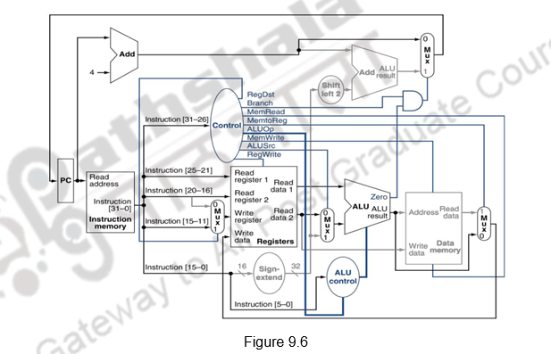
Now, we shall trace the execution flow for different types of instructions and see what control signals have to be activated. Let us consider the execution of an R type instruction first. For all these instructions, the source register fields are Rs and Rt, and the destination register field is Rd. The various operations that take place for an arithmetic / logical operation with register operands are:
- The instruction is fetched from the code memory
- Since the Branch control signal is set to 0, the PC is unconditionally replaced with PC + 4
- The two registers specified in the instruction are read from the register file
- The ALU operates on the data read from the register file, using the function code (bits 5:0, which is the funct field, of the instruction) to generate the ALU function
- The ALUSrc control signal is deasserted, indicating that the second operand comes from a register
- The ALUOp field for R-type instructions is set to 10 to indicate that the ALU control should be generated from the funct field
- The result from the ALU is written into the register file using bits 15:11 of the instruction to select the destination register
- The RegWrite control signal is asserted and the RegDst control signal is made 1, indicating that Rd is the destination register
- The MemtoReg control signal is made 0, indicating that the value fed to the register write data input comes from the ALU
Furthermore, an R-type instruction writes a register (RegWrite = 1), but neither reads nor writes data memory. So, the MemRead and MemWrite control signals are set to 0. These operations along with the required control signals are indicated in Figure 9.6.
Similarly, we can illustrate the execution of a load word, such as lw t2). Figure 9.7 shows the active functional units and asserted control lines for a load. We can think of a load instruction as operating in five steps:
- The instruction is fetched from the code memory
- Since the Branch control signal is set to 0, the PC is unconditionally replaced with PC + 4
- A register ($t2) value is read from the register file
- The ALU computes the sum of the value read from the register file and the sign-extended, lower 16 bits of the instruction (offset)
- The ALUSrc control signal is asserted, indicating that the second operand comes from the sign extended operand
- The ALUOp field for R-type instructions is set to 00 to indicate that the ALU should perform addition for the address calculation
- The sum from the ALU is used as the address for the data memory and a data memory read is performed
- The MemRead is asserted and the MemWrite control signals is set to 0
- The result from the ALU is written into the register file using bits 20:16 of the instruction to select the destination register
- The RegWrite control signal is asserted and the RegDst control signal is made 0, indicating that Rt is the destination register
- The MemtoReg control signal is made 1, indicating that the value fed to the register write data input comes from the data memory

A store instruction is similar to the load for the address calculation. It finishes in four steps The control signals that are different from load are:
- MemWrite is 1 and MemRead is 0
- RegWrite is 0
- MemtoReg and RegDst are X’s (don’t cares)
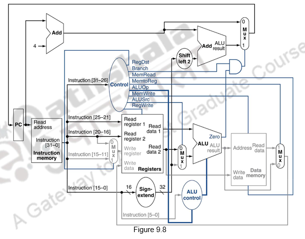
The branch instruction is similar to an R-format operation, since it sends the Rs and Rt registers to the ALU. The ALUOp field for branch is set for a subtract (ALU control = 01), which is used to test for equality. The MemtoReg field is irrelevant when the RegWrite signal is 0. Since the register is not being written, the value of the data on the register data write port is not used. The Branch control signal is set to 1. The ALU performs a subtract on the data values read from the register file. The value of PC + 4 is added to the sign-extended, lower 16 bits of the instruction (offset) shifted left by two; the result is the branch target address. The Zero result from the ALU is used to decide which adder result to store into the PC. The control signals and the data flow for the Branch instruction is shown in Figure 9.8.
Now, to the subset of instructions already discussed, we shall add a jump instruction. The jump instruction looks somewhat similar to a branch instruction but computes the target PC differently and is not conditional. Like a branch, the low order 2 bits of a jump address are always 00. The next lower 26 bits of this 32-bit address come from the 26-bit immediate field in the instruction, as shown in Figure 9.9. The upper 4 bits of the address that should replace the PC come from the PC of the jump instruction plus 4. Thus, we can implement a jump by storing into the PC the concatenation of the upper 4 bits of the current PC + 4 (these are bits 31:28 of the sequentially following instruction address), the 26-bit immediate field of the jump instruction and the bits 00.

Figure 9.10 shows the addition of the control for jump added to the previously discussed control.
An additional multiplexor is used to select the source for the new PC value, which is either the incremented PC (PC + 4), the branch target PC, or the jump target PC. One additional control signal is needed for the additional multiplexor. This control signal, called Jump, is asserted only when the instruction is a jump—that is, when the opcode is 2.

Since we have assumed that all the instructions get executed in one clock cycle, the longest instruction determines the clock period. For the subset of instructions considered, the critical path is that of the load, which takes the following path Instruction memory ® register file ® ALU ® data memory ® register file
The single cycle implementation may be acceptable for this simple instruction set, but it is not feasible to vary the period for different instructions, for eg. Floating point operations. Also, since the clock cycle is equal to the worst case delay, there is no point in improving the common case, which violates the design principle of making the common case fast. In addition, in this single-cycle implementation, each functional unit can be used only once per clock. Therefore, some functional units must be duplicated, raising the cost of the implementation. A single-cycle design is inefficient both in its performance and in its hardware cost. These shortcomings can be avoided by using implementation techniques that have a shorter clock cycle—derived from the basic functional unit delays—and that require multiple clock cycles for each instruction. In the next module, we will look at another implementation technique, called pipelining, that uses a datapath very similar to the single-cycle datapath, but is much more efficient.
Next, we shall briefly discuss another type of control, viz. microprogrammed control. In the case of hardwired control, we saw how all the control signals required inside the CPU can be generated using hardware. There is an alternative approach by which the control signals required inside the CPU can be generated. This alternative approach is known as microprogrammed control unit. In microprogrammed control unit, the logic of the control unit is specified by a microprogram. A microprogram consists of a sequence of instructions in a microprogramming language. These are instructions that specify microoperations. A microprogrammed control unit is a relatively simple logic circuit that is capable of (1) sequencing through microinstructions and (2) generating control signals to execute each microinstruction.
The concept of microprogram is similar to computer program. In computer program the complete instructions of the program is stored in main memory and during execution it fetches the instructions from main memory one after another. The sequence of instruction fetch is controlled by the program counter (PC). Microprograms are stored in microprogram memory and the execution is controlled by the microprogram counter ( PC). Microprograms consist of microinstructions which are nothing but strings of 0’s and 1’s. In a particular instance, we read the contents of one location of microprogram memory, which is nothing but a microinstruction. Each output line (data line) of microprogram memory corresponds to one control signal. If the contents of the memory cell is 0, it indicates that the signal is not generated and if the contents of memory cell is 1, it indicates the generation of the control signal at that instant of time.
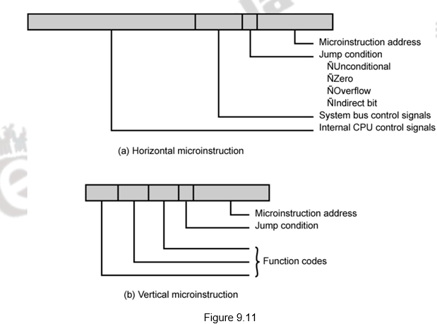
There are basically two types of microprogrammed control – horizontal organization and vertical organization. In the case of horizontal organization, as mentioned above, you can assume that every bit in the control word corresponds to a control signal. In the case of a vertical organization, the signals are grouped and encoded in order to reduce the size of the control word. Normally some minimal level of encoding will be done even in the case of horizontal control. The fields will remain encoded in the control memory and they must be decoded to get the individual control signals. Horizontal organization has more control over the potential parallelism of operations in the datapath; however, it uses up lots of control store. Vertical organization, on the other hand, is easier to program, not very different from programming a RISC machine in assembly language, but needs extra level of decoding and may slow the machine down. Figure 9.11 shows the two formats.
The different terminologies related to microprogrammed control unit are:
Control Word (CW) : Control word is defined as a word whose individual bits represent the various control signal. Therefore each of the control steps in the control sequence of an instruction defines a unique combination of 0s and 1s in the CW. A sequence of control words (CWs) corresponding to the control sequence of a machine instruction constitute the microprogram for that instruction. The individual control words in this microprogram are referred to as microinstructions. The microprograms corresponding to the instruction set of a computer are stored in a special memory that will be referred to as the microprogram memory or control store. The control words related to all instructions are stored in the microprogram memory.
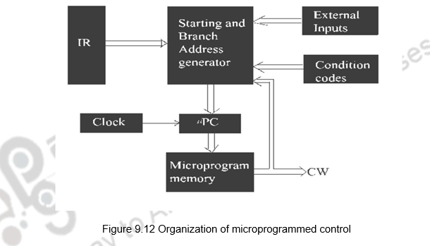
The control unit can generate the control signals for any instruction by sequencially reading the CWs of the corresponding microprogram from the microprogram memory. To read the control word sequentially from the microprogram memory a microprogram counter ( PC) is needed. The basic organization of a microprogrammed control unit is shown in the Figure 3.7. The starting address generator block is responsible for loading the starting address of the microprogram into the PC everytime a new instruction is loaded in the IR. The PC is then automatically incremented by the clock, and it reads the successive microinstruction from memory. Each microinstruction basically provides the required control signal at that time step. The microprogram counter ensures that the control signal will be delivered to the various parts of the CPU in correct sequence.
We have some instructions whose execution depends on the status of condition codes and status flag, as for example, the branch instruction. During branch instruction execution, it is required to take the decision between alternative actions. To handle such type of instructions with microprogrammed control, the design of the control unit is based on the concept of conditional branching in the microprogram. In order to do that, it is required to include some conditional branch microinstructions. In conditional microinstructions, it is required to specify the address of the microprogram memory to which the control must be directed to. It is known as the branch address. Apart from the branch address, these microinstructions can specify which of the states flags, condition codes, or possibly, bits of the instruction register should be checked as a condition for branching to take place.
In a computer program we have seen that execution of every instruction consists of two parts – fetch phase and execution phase of the instruction. It is also observed that the fetch phase of all instruction is the same. In a microprogrammed control unit, a common microprogram is used to fetch the instruction. This microprogram is stored in a specific location and execution of each instruction starts from that memory location. At the end of the fetch microprogram, the starting address generator unit calculates the appropriate starting address of the microprogram for the instruction which is currently present in IR. After that the PC controls the execution of microprogram which generates the appropriate control signals in the proper sequence. During the execution of a microprogram, the PC is incremented everytime a new microinstruction is fetched from the microprogram memory, except in the following situations :
1. When an End instruction is encountered, the PC is loaded with the address of the first CW in the microprogram for the next instruction fetch cycle.
2. When a new instruction is loaded into the IR, the PC is loaded with the starting address of the microprogram for that instruction.
3. When a branch microinstruction is encountered, and the branch condition is satisfied, the PC is loaded with the branch address.
The organization of a microprogrammed control unit is given in Figure 9.12.
Microprogrammed control pros and cons
- Ease of design
- Flexibility
- Easy to adapt to changes in organization, timing, technology
- Can make changes late in design cycle, or even in the field
- Can implement very powerful instruction sets (just more control memory)
- Generality
- Can implement multiple instruction sets on same machine
- Can tailor instruction set to application.
- Compatibility
- Many organizations, same instruction set
- Costly to implement
- Slow
To summarize, we have looked at the control signals needed for the MIPS architecture for implementing a subset of instructions. We have looked at the control flow for the Arithmetic/logical instructions, Load/Store instructions, Branch instruction and jump instruction. We also looked at the concepts related to microprogrammed control.
Web Links / Supporting Materials
- Computer Organization and Design – The Hardware / Software Interface, David A. Patterson and John L. Hennessy, 4th.Edition, Morgan Kaufmann, Elsevier, 2009.
- Computer Organization, Carl Hamacher, Zvonko Vranesic and Safwat Zaky, 5th.Edition, McGraw- Hill Higher Education, 2011.